 |
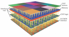
| Figure 1. A three-dimensional integrated circuit, made possible with carbon nanotubes (CNTs). The circuit senses and classifies ambient gases using a multilayered stack of devices that are connected by platinum wires known as interlayer vias. In the top layer, roughly 1 million CNT field-effect transistors (FETs) register a change in electrical resistance when the gas molecules adsorb on a CNT. The second layer hosts memory cells that read and store the signals created by the FETs just above them. The third layer contains another million FETs that process the sensor data and implement a machine-learning algorithm to identify the type of gas picked up. Conventional silicon CMOS circuitry on the bottom acts as an interface to external devices. (Adapted from ref. 2.) |
Topics: Carbon Nanotubes, Computer Engineering, Nanotechnology, Quantum Mechanics
In 2013 graduate student Max Shulaker, his adviser Subhasish Mitra, Philip Wong, and their Stanford University colleagues built the first computer made entirely of carbon nanotube (CNT) field-effect transistors (FETs). 1 The achievement was eagerly anticipated. Even before their first incorporation into FETs in 1998, CNTs had been touted as a superior substitute for the silicon channel that shuttles current between the traditional FET’s source and drain electrodes.
The intrinsic thinness of single-wall CNTs—essentially graphene sheets rolled into hollow cylinders a nanometer wide—enables superb control over power dissipation in the transistor’s off state and allows the transistor to switch off and on with much lower energy consumption than is possible with any other material. Moreover, thanks to that one-dimensionality, which suppresses scattering, charge carriers in CNTs have a much higher velocity for a given electric field than in Si. (See the article by Phaedon Avouris, Physics Today, January 2009, page 34.)
The 2013 computer was modest: It contained fewer than 200 FETs, ran at a clock speed of just 1 kHz, and implemented a single instruction. Nonetheless, the instruction was a conditional statement that qualified the computer as “Turing complete,” able to make any calculation given enough memory and time. The achievement also reassured Shulaker, now a professor at MIT, and his Stanford colleagues that CNTs could form the foundation for a much more complex system.
The researchers have now built a prototype system that embodies a vision of a transformative computer architecture—one in which computing, data storage, and input and output technologies are each fabricated into two-dimensional layers that are built up into a 3D integrated circuit.2 Shown schematically in figure 1, the circuit consists of more than 2 million CNT FETs and more than 1 million memory cells. The components are divided among three layers—stacked on the same chip atop a layer of Si CMOS circuitry and interconnected by a forest of fine platinum wires.
The carbon nanotube integrated circuit goes three-dimensional R. Mark Wilson, Physics Today
Comments