 |
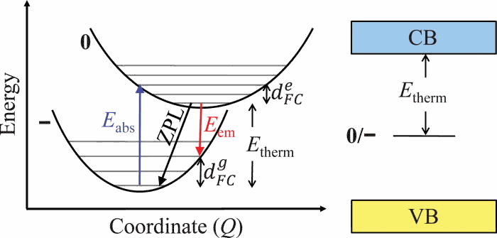
| Configuration coordinate diagram, showing important energies and optical transitions. For this example, Etherm gives the acceptor level relative to the CBM. Citation: J. Appl. Phys. 119, 181101 (2016); http://dx.doi.org/10.1063/1.4948245 |
Topics: Education, Nanotechnology, Semiconductor Technology, STEM
Abstract
Point defects affect or even completely determine physical and chemical properties of semiconductors. Characterization of point defects based on experimental techniques alone is often inconclusive. In such cases, the combination of experiment and theory is crucial to gain understanding of the system studied. In this tutorial, we explain how and when such comparison provides new understanding of the defect physics. More specifically, we focus on processes that can be analyzed or understood in terms of configuration coordinate diagrams of defects in their different charge states. These processes include light absorption, luminescence, and nonradiative capture of charge carriers. Recent theoretical developments to describe these processes are reviewed.
Introduction
Every material contains defects; perfect materials simply do not exist. While it may cost energy to create a defect, configurational entropy renders it favorable to incorporate a certain concentration of defects, since this lowers the free energy of the system.1 Therefore, even in equilibrium, we can expect defects to be present; kinetic limitations sometimes lead to formation of additional defects. Note that all of these considerations also apply to impurities that are unintentionally present in the growth or processing environment. Of course, impurities are often intentionally introduced to tailor the properties of materials. Doping of semiconductors with acceptors and donors is essential for electronic and optoelectronic applications. In the following, we will use the word “defect” as a generic term to cover both intrinsic defects (vacancies, self-interstitials, and antisites) and impurities.
Since defects are unavoidable, we must consider the effects they have on the properties of materials. These effects can be considerable, to the point of determining the functionality of the material, as in p- or n-type doping. Point defects play a key role in diffusion: virtually all diffusion processes are assisted by point defects. Defects are often responsible for degradation of a device. Even in the absence of degradation, defects can limit the performance of a device. Compensation by native point defects can decrease the level of doping that can be achieved. Defects with energy levels within the band gap can act as recombination centers, impeding carrier collection in a solar cell or light emission from a light-emitting diode. Sometimes, these effects can be used to advantage: luminescence centers in wide-band-gap materials can be used to emit light at specified wavelengths; or single-spin centers (such as the nitrogen–vacancy (NV) center in diamond) can act as an artificial atom and serve as a qubit in a quantum information system.2,3 Finally, sometimes, one deliberately wants to grow materials with many defects. Examples are materials for ultrafast optoelectronic switches or semiconductors used to optically generate THz pulses, where defect densities should be large enough so that carrier lifetimes are as short as a few picoseconds.4
Journal of Applied Physics:
Tutorial: Defects in semiconductors—Combining experiment and theory
Audrius Alkauskas1, Matthew D. McCluskey2 and Chris G. Van de Walle3,a)
Comments