nanotechnology (84)

John E. Hodge...

john-e.-hodge-235x300.png
John E. Hodge, African American Registry (link below)


Topics: African Americans, Chemistry, Diversity in Science, Nanotechnology


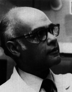
John Edward Hodge was born on this date (October 12) in 1914. He was an African American chemist.

From Kansas City, Kansas he was the son of Anna Belle Jackson and John Alfred Hodge. His active mind found certain games and sports to be a challenge. He won a number of model airplane contests in Kansas City. He became an expert at billiards in college, and later in Peoria. Chess was another fascination for John, his father, John Alfred, and his son, John Laurent. He graduated from Sumner High School in 1932 and got his A.B. degree in 1936. Hodge received his M.A. in 1940 from the University of Kansas where he was elected to the PI-ii Beta Kappa scholastic society and the Pi Mu Epsilon honorary mathematics organization. He did his postgraduate studies at Bradley University between 1946 and 1960 and received a diploma from the Federal Executive Institute, Charlottesville, VA in 1971.

Hodges career began as oil chemist in Topeka, Kansas at the Department of Inspections. He was also a professor of chemistry at Western University, Quindaro, KS. In 1941 he began nearly 40 years of service at the USDA Nonhem Regional Research Center in Peoria, IL; where he retired in 1980. During that time (1972) he was visiting professor of chemistry at the University of Campinas, Sao Paulo, Brazil. He also received a Superior Service Award at Washington, D.C., from the U.S. Department of Agriculture in 1953, and two research team awards also. He was chairman of the Division of Carbohydrate Chemistry of the American Chemical Society in 1964, and was an active member of the cereal chemists and other scientific organizations. After retirement Hodge was an adjunct chemistry professor at Bradley University in 1984-85.

Hodge encouraged young black college students to study chemistry. He made tours of historically Black colleges in the South to assess their laboratory capabilities, and recruited summer interns for research experiences. Hodge was on the board of directors of Carver Community Center from 1952 to 1958. In 1953 he was secretary of the Citizens Committee for Peoria Public Schools; as well as secretary for the Mayor's Commission for Senior Citizens, 1982-85. Hodge was an advisory board member at the Central Illinois Agency for the Aging in 1975. John Hodge died on January 3, 1996.


African American Registry: John E. Hodge

Read more…

Dr. Bettye Washington Greene...

q237hs45t_thumb_large.jpeg
Science History Institute: Dr. Bettye Washington Greene


Topics: African Americans, Chemistry, Diversity in Science, Nanotechnology, Women in Science


American Chemical Society: Nanotechnology


Bettye Greene was born on March 20, 1935 in Fort Worth, Texas and earned her B.S. from the Tuskegee Institute in 1955 and her Ph.D. from Wayne State University in 1962, studying under Wilfred Heller. She began working for Dow in 1965 in the E.C. Britton Lab, where she specialized in Latex products. According to her former colleague, Rudolph Lindsey, Dr. Greene served as a Consultant on Polymers issues in the Saran Research Laboratory and the Styrene Butadiene (SB) Latex group often utilized her expertise and knowledge. In 1970, Dr. Greene was promoted to the position of senior research chemist. She was subsequently promoted to the position of senior research specialist in 1975.

In addition to her work at Dow, Bettye Greene was active in community service in Midland and was a founding member of the Delta Sigma Theta Sorority, Inc., a national service group for African-American women (actually, more likely one of the alumni chapters). Greene retired from Dow in 1990 and passed away in Midland on June 16, 1995. [1]


*****


Her doctoral dissertation, "Determination of particle size distributions in emulsions by light scattering" was published in 1965.

Patents:

4968740: Latex-based adhesive prepared by emulsion polymerization
4609434: Composite sheet prepared with stable latexes containing phosphorus surface groups
4506057: Stable latexes containing phosphorus surface groups [2]


Spouse: Veteran Air Force Captain William Miller Greene in 1955, she attended Wayne State University in Detroit, where she earned her Ph.D. in physical chemistry working with Wilfred Heller.

Children: Willetta Greene Johnson, Victor M. Greene; Lisa Kianne Greene [2]


1. Science History Institute Digital Collections: Dr. Bettye Washington Greene
2. Wikipedia/Bettye_Washington_Greene

Read more…

Dr. Dorothy Lavinia Brown...

Dorothy_Lavinia_Brown__public_domain_-1.png
Dr. Dorothy Lavinia Brown
Image Ownership: Public Domain


Topics: African Americans, Diversity in Science, Medical Science, Nanotechnology, Women in Science


Understanding Nano: Nanotechnology in Medicine

Dr. Dorothy Lavinia Brown was a medical pioneer, educator, and community leader. In 1948-1949 Brown became the first African American female appointed to a general surgery residency in the de jure racially segregated South. In 1956 Brown became the first unmarried woman in Tennessee authorized to be an adoptive parent, and in 1966 she became the first black woman representative to the state legislature in Tennessee.

Brown was born in Philadelphia, Pennsylvania on January 7, 1919. Within weeks after she was born, Brown’s unmarried mother Edna Brown moved to upstate New York and placed her five-month-old baby daughter in the predominantly white Troy Orphan Asylum (later renamed Vanderhyden Hall) in Troy, New York. Brown was a demonstrably bright child, and became interested in medicine after she had a tonsillectomy at age five.

When Brown was 13 years old her estranged mother reclaimed her. Subsequently, however, Brown would run away from her mother five times, returning to the orphanage each time. During her teenage years Brown worked at a Chinese laundry, and also as a mother’s helper for Mrs. W.F. Jarrett, who encouraged her desire to become a physician. At age 15, the last time Brown ran away from her mother, she enrolled herself at Troy High School. Realizing that Brown had no place to stay, the principal arranged for Brown to live with Lola and Samuel Wesley Redmon, foster parents who became a major influence in her life and from whom Brown received the security and support she needed until she graduated at the top of her high school class in 1937. Awarded a four-year scholarship by the Troy Conference Methodist Women, in 1941 Brown graduated second in her class from Bennett College in Greensboro, North Carolina.

During World War II Brown worked as an inspector for the Army Ordnance Department in Rochester, New York. In 1944 Brown began studying medicine at the Meharry Medical College in Nashville, Tennessee, receiving her Medical Degree in 1948. After serving a year-long residency internship at Harlem Hospital in New York City, Brown returned to Meharry’s George Hubbard Hospital in 1949 for her five-year residency, becoming Professor of Surgery in 1955.

In the mid-1950s an unmarried patient of Brown’s pleaded with her to adopt her newborn daughter, and in 1956 Brown became the first known single woman to adopt a child in the state of Tennessee. As a tribute to her foster mother, Brown named her daughter Lola Denise Brown.

From 1966 to 1968 Brown served in the Tennessee House of Representatives, where she introduced a controversial bill to reform the state’s abortion law to allow legalized abortions in cases of incest and rape. Brown also co-sponsored legislation that recognized Negro History Week, which later expanded to Black History Month.


The Black Past: Dr. Dorothy Lavinia Brown

Read more…

Dr. Gladys W. Royal...

THE_A%2526T_COLLEGE_REGISTER_1961_Gladys_Royal%252C_W._E._Reed%252C_R._L._Satoera%252C_George_Royal.jpg
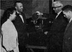
Dr. Gladys Royal (left), Dr. W. E. Reed (left center), R. L. Satoera (right center) and Dr. George Royal (right), with x-ray equipment, North Carolina A&T College, 1961

By THE AGRICULTURAL AND TECHNICAL, COLLEGE, GREENSBORO, N. C. - THE A&T COLLEGE REGISTER, VOLUME XXXII, No. 8 , FRIDAY, JANUARY 13, 1961, Public Domain, https://commons.wikimedia.org/w/index.php?curid=42353373


Topics: African Americans, Diversity in Science, Biochemistry, Nanotechnology, Women in Science

See: Biochemistry and structural DNA nanotechnology: an evolving symbiotic relationship.


Gladys W. Royal (August 29, 1926 – November 9, 2002) is one of a small number of early African-American biochemists. Part of one of the few African-American husband-and-wife teams in science, Gladys worked with George C. Royal on research supported by the United States Atomic Energy Commission. She later worked for many years as principal biochemist at the Cooperative State Research Service of the U.S. Department of Agriculture. Royal was also active in the civil rights movement in Greensboro, North Carolina.

Royal was born Gladys Geraldine Williams on August 29, 1926, in Dallas, Texas. She graduated from Dillard University with a B.Sc. at the age of 18 in 1944. She married George C. Royal in 1947.

Royal accompanied her husband to Tuskegee, Alabama, where he taught microbiology in 1947-1948, to Ohio State University and Ohio Agricultural Experiment Station, where he was a research assistant from 1948 to 1952, and to North Carolina Agricultural and Technical College in Greensboro where he became an assistant professor of Bacteriology in 1952. At Tuskegee and Ohio State she took classes; by 1953, she was sufficiently qualified to become a professor of chemistry at North Carolina Agricultural and Technical College in Greensboro.

In 1954, Royal received her M.Sc. in organic chemistry from Tuskegee. She had also taken classes at the University of Wisconsin and at Ohio State University, from which she received her Ph.D. in 1954. Her thesis, The Influence of Rations Containing Sodium Acetate and Sodium Propionate on the Composition of Tissues From Feeder Lambs, involved experimental work in flavor chemistry, testing the effects of various feed regimens on the taste of meat.

In the late 1950s and early 1960s, the Royals collaborated on important research including that funded by the United States Atomic Energy Commission involving bone marrow transplants to treat radiation overdoses. Their work had direct relevance to cancer treatment, which used high doses of radiation and could cause tissue damage. It also reflected Cold war fears of possible nuclear attack.

African-American husband-and-wife teams in science were extremely rare in the early and mid-20th century due to the social, educational and economic climate regarding African Americans in the United States.

The Royals had six children: George Calvin Royal III, Geraldine Gynnette Royal, Guericke Christopher Royal, jazz musician Gregory Charles Royal, Michelle Renee McNear, and Eric Marcus Royal.


Source: Wikipedia/Gladys_W._Royal

Read more…

Dr. Mark Dean, repost...

mark-dean.jpg
Dr. Mark Dean - Biography.com


Topics: African Americans, Computer Science, Electrical Engineering, Nanotechnology, STEM


This is admittedly a repost that appears during the month of February. The popular celebrities of sports, music and "reality" television dominate the imaginations of youth from all cultural backgrounds. It's important especially that African American children see themselves doing and making a living at STEM careers. A diverse workforce doesn't just "happen." Like the opposite of diversity - segregation - has to be intentionally planned and executed. For our country to survive and compete in nanotechnology, it MUST be a priority.

Computer scientist and engineer Mark Dean is credited with helping develop a number of landmark technologies, including the color PC monitor, the Industry Standard Architecture system bus and the first gigahertz chip.

Synopsis

Born in Jefferson City, Tennessee, in 1957, computer scientist and engineer Mark Dean helped develop a number of landmark technologies for IBM, including the color PC monitor and the first gigahertz chip. He holds three of the company's original nine patents. He also invented the Industry Standard Architecture system bus with engineer Dennis Moeller, allowing for computer plug-ins such as disk drives and printers.

Early Life and Education

Computer scientist and inventor Mark Dean was born on March 2, 1957, in Jefferson City, Tennessee. Dean is credited with helping to launch the personal computer age with work that made the machines more accessible and powerful.

From an early age, Dean showed a love for building things; as a young boy, Dean constructed a tractor from scratch with the help of his father, a supervisor at the Tennessee Valley Authority. Dean also excelled in many different areas, standing out as a gifted athlete and an extremely smart student who graduated with straight A's from Jefferson City High School. In 1979, he graduated at the top of his class at the University of Tennessee, where he studied engineering.

Innovation with IBM

Not long after college, Dean landed a job at IBM, a company he would become associated with for the duration of his career. As an engineer, Dean proved to be a rising star at the company. Working closely with a colleague, Dennis Moeller, Dean developed the new Industry Standard Architecture (ISA) systems bus, a new system that allowed peripheral devices like disk drives, printers and monitors to be plugged directly into computers. The end result was more efficiency and better integration.

But his groundbreaking work didn't stop there. Dean's research at IBM helped change the accessibility and power of the personal computer. His work led to the development of the color PC monitor and, in 1999, Dean led a team of engineers at IBM's Austin, Texas, lab to create the first gigahertz chip—a revolutionary piece of technology that is able to do a billion calculations a second.

In all, Dean holds three of the company's original nine patents for the IBM personal computer - a market the company helped create in 1981 and, in total, has more 20 patents associated with his name.


Biography.com: Mark Dean, Ph.D.

Read more…

Dr. Jessica Isabelle Price...

Dr_Jessie_Isabelle_Price-560x416.jpg
Image Source: Darq Side Nerdettes dot com


Topics: African Americans, Diversity in Science, Microbiology, Nanotechnology, Women in Science


January 1, 1930 - November 12, 2015

Dr. Jessie Isabelle Price was a microbiologist best known for developing vaccines for common avian diseases.

Born January 1, 1930, Dr. Price was raised by her single mother who encouraged her children to work hard in school. And that advice paid off when Dr. Price graduated from her predominately white school and was accepted into Cornell University.

But just make sure she was extra ready for college, Dr. Price moved with her mother to Ithaca, New York to take advanced classes in math and English for a year. Fortunately, she didn’t have to worry about paying tuition since her New York residency qualified her for waived tuition fees.

Too bad it didn’t work that way at Cornell.

Dr. Price wanted to be a physician, but couldn’t because of the cost. Instead, she earned a Bachelor of Science in in microbiology from the College of Agriculture in 1953.

Her mentor, Dorsey Buner, suggested she take on post-grad studies, but once again, a lack of sufficient funds cut off her access.

To get around this, Dr. Price worked as a laboratory tech at the Poultry Disease Research Farm in the Veterinary College at Cornell to save post-grad money.

She eventually gained research assistant support from 1956 to 1959 and earned a Masters in veterinary bacteriology, pathology, and parasitology in 1958. Then, she went on to earn her doctorate in 1959 under the supervision of Bruner.

Her dissertation was the start of her path to creating a vaccine. She isolated and reproduced the bacterium, Pasteurella anatipestifer, in white pekin (“Long Island”) ducklings infected with a disease that was a major killer in duck farms.

Dr. Price joined the Cornell Duck Research Laboratory, and worked there from 1959 to 1977 and taught at Long Island University, where she became an adjunct professor.

In 1964, Ebony magazine featured Dr. Price and her work in an extensive photo-essay describing and showing her work on vaccine development, in the Duck Research Laboratory and on the farms.

She was awarded a National Science Foundation travel grant to present her findings at the International Congress for Microbiology in Moscow in 1966.


Darq Side Nerdettes - Black Women in STEAM: Dr. Jessie Isabelle Price

Read more…

Environmental Justice and ENPs...


Topics: African Americans, Diversity, Diversity in Science, Ecology, Environment, Nanotechnology


Abstract

The production and use of Engineered Nanoparticles (ENPs) or materials containing ENPs has increased astonishingly, leading to increased exposure to workers and consumers. The invention and applications of new materials either create new opportunities or pose new risks and uncertainties. The uncertainties concerning application of ENPs are posing disturbances to the ecosystem and human health. This review first addresses in vitro and in vivo studies conducted on the toxicity of ENPs to animals and humans. Ethical justifications are provided specially with reference to Intergenerational Justice (IRG-J) and Ecological Justice (EC-J). The social benefits and burdens of ENPs are identified for present and future generations. Some mitigation approaches for combating the potential risks posed by ENPs are proposed. Finally, suggestions for the safe handling of ENPs in future are proposed in the review.
 
*****

The term nanotechnology refers to the science of investigating and manipulating materials at atomic, molecular and macromolecular scale. (Sudarenko, 2013). Nanoparticles (NPs) are known to occur naturally (e.g., volcanic ash and forest fires), accidentally (i.e., unintended human activities) and anthropogenic (e.g., cosmetics and other consumer products). Engineered nanomaterials (ENMs) or engineered nanoparticles (ENPs) are man made materials produced deliberately for different industrial applications and most commonly having dimension from 1 to 100 nm (Auffan et al., 2009). It is widely acknowledged in the scientific community that ENPs have enormous potential to transform industrial processes in the future thereby shaping how the society and the global economy will function. They have several industrial and domestic applications in consumer products, cosmetics, agriculture, soil and groundwater remediation, electronics, energy storage, biomedical and transportation (Besha et al., 2018; Boldrin et al., 2014).

Engineered nanomaterials (ENMs) or engineered nanoparticles (ENPs) are man made materials produced deliberately for different industrial applications and most commonly having dimension from 1 to 100 nm (Auffan et al., 2009). It is widely acknowledged in the scientific community that ENPs have enormous potential to transform industrial processes in the future thereby shaping how the society and the global economy will function. They have several industrial and domestic applications in consumer products, cosmetics, agriculture, soil and groundwater remediation, electronics, energy storage, biomedical and transportation (Besha et al., 2018; Boldrin et al., 2014).


Sustainability and environmental ethics for the application of engineered nanoparticles
Abreham Tesfaye Beshaa, Yanju Liubc, Dawit N. Bekelebc, Zhaomin Dongd, Ravi Naidubc, Gebru Neda Gebremariama

*****


“Poison is the wind that blows from the north and south and east.” Marvin Gaye wasn’t an environmental scientist, but his 1971 single “Mercy Mercy Me (The Ecology)” provides a stark and useful environmental analysis, complete with warnings of overcrowding and climate change. The song doesn’t explicitly mention race, but its place in Gaye’s What’s Going On album portrays a black Vietnam veteran, coming back to his segregated community and envisioning the hell that people endure.

Gaye’s prophecies relied on the qualitative data of storytelling—of long-circulated anecdotes and warnings within black communities of bad air and water, poison, and cancer. But those warnings have been buttressed by study after study indicating that people of color face disproportionate risks from pollution, and that polluting industries are often located in the middle of their communities.

Late last week, even as the Environmental Protection Agency and the Trump administration continued a plan to dismantle many of the institutions built to address those disproportionate risks, researchers embedded in the EPA’s National Center for Environmental Assessment released a study indicating that people of color are much more likely to live near polluters and breathe polluted air. Specifically, the study finds that people in poverty are exposed to more fine particulate matter than people living above poverty. According to the study’s authors, “results at national, state, and county scales all indicate that non-Whites tend to be burdened disproportionately to Whites.”


Trump's EPA Concludes Environmental Racism Is Real
A new report from the Environmental Protection Agency finds that people of color are much more likely to live near polluters and breathe polluted air—even as the agency seeks to roll back regulations on pollution.
Vann R. Newkirk, The Atlantic

Read more…

Nanotech and Business...

JSNN.JPG
Joint School of Nanoscience and Nanoengineering: Facebook


Topics: African Americans, Diversity, Diversity in Science, Economics, Nanotechnology


Historically Black Colleges & Universities (HBCUs) should pursue research in the nanotech sector. Other universities are leveraging significant funding to lead the way in nanotechnology research. For instance, the Institute for Nanotechnology was established as an umbrella organization for the multi-million dollar nanotechnology research efforts at Northwestern University. The role of the Institute is to support meaningful efforts in nanotechnology, house state-of-the-art nanomaterials characterization facilities, and support individual and group efforts aimed at addressing and solving key problems in nanotechnology.As part of this effort, a $34 million, 40,000 square foot state-of-the-art Center for Nanofabrication and Molecular Self-Assembly was constructed on the Evanston, Illinois campus. The new facility, which was anchored by a $14 million grant from the Department of Health and Human Services, is one of the first federally funded facilities of its kind in the United States and home to the Institute headquarters.

Since you asked...

The Nano School

Nanotechnology is often referred to as convergent technology because it utilizes knowledge from a diverse array of disciplines including biology, chemistry, physics, engineering, and technology. JSNN has six research focus areas—nanobioscience, nanometrology, nanomaterials (with special emphasis on nanocomposite materials), nanobioelectronics, nanoenergy, and computational nanotechnology.

Our Mission

The Joint School of Nanoscience and Nanoengineering (JSNN) mission is to be a catalyst for breakthrough innovations that provides high-impact academic, industry and government research outcomes.

Our Vision

The Joint School of Nanoscience and Nanoengineering (JSNN) is a collaboration between two high research universities: North Carolina A&T State University (NC A&T SU) and The University of North Carolina at Greensboro (UNCG). Collaboration will always be a core part of JSNN’s DNA. JSNN will constantly seek out strategic collaborations with other academic institutions, industry and government organizations as a catalyst for continuing to produce research breakthroughs.

To achieve the mission, JSNN recruits students that are the best and brightest men and women from a variety of disciplines to conduct advanced research in Nanoengineering and Nanoscience. Students are challenged to choose a research area that is expected to provide significant benefit to mankind. Beyond becoming exceptional researchers, students will develop leadership and communication skills that will make them an exceptional asset in any academic, industry or government organization.

JSNN is also catalyst for economic development. The Southeastern Nanotechnology Infrastructure Corridor (SENIC) was created as a partnership between Georgia Tech and JSNN, a collaboration of NC A&T and UNCG. SENIC combines the infrastructure strengths of both Georgia Tech and the JSNN to provide academic, industry and government users affordable access to one of the largest and most modern Nano-fabrication and Nano-characterization tool sets in the country.
Read more…

Nanotechnology and People...

F0C0E23E-803B-45BF-9B9A-30B6076483DF-650x431.jpeg
Image Source: Disruption Hub (link below)


Topics: African Americans, Diversity, Diversity in Science, Nanotechnology


In the 1950s, physicist Richard Feynman suggested that more could be learned about materials by reducing them to their smallest possible form. This idea laid the foundations for nanotechnology – the study of matter at an atomic or molecular level. Almost 70 years down the line, however, and the field is still in the developmental stages. Nonetheless, the disruptive potential of nanotechnology is so vast that it’s well worth being aware of the technology’s trajectory. The research area is now a broad umbrella term for numerous different branches and projects. But what does it mean for businesses, and what are the obstacles to adoption?

Any technological advance is a disruption. We get the term Luddites from essentially a backlash to economic conditions in England brought on by endless war with France:

The Luddite disturbances started in circumstances at least superficially similar to our own. British working families at the start of the 19th century were enduring economic upheaval and widespread unemployment. A seemingly endless war against Napoleon’s France had brought “the hard pinch of poverty,” wrote Yorkshire historian Frank Peel, to homes “where it had hitherto been a stranger.” Food was scarce and rapidly becoming more costly. Then, on March 11, 1811, in Nottingham, a textile manufacturing center, British troops broke up a crowd of protesters demanding more work and better wages.

That night, angry workers smashed textile machinery in a nearby village. Similar attacks occurred nightly at first, then sporadically, and then in waves, eventually spreading across a 70-mile swath of northern England from Loughborough in the south to Wakefield in the north. Fearing a national movement, the government soon positioned thousands of soldiers to defend factories. Parliament passed a measure to make machine-breaking a capital offense.

But the Luddites were neither as organized nor as dangerous as authorities believed. They set some factories on fire, but mainly they confined themselves to breaking machines. In truth, they inflicted less violence than they encountered. In one of the bloodiest incidents, in April 1812, some 2,000 protesters mobbed a mill near Manchester. The owner ordered his men to fire into the crowd, killing at least 3 and wounding 18. Soldiers killed at least 5 more the next day.

What the Luddites Really Fought Against, Richard Conniff, Smithsonian Magazine

The Internet is an example of technology causing displacement and disruption. The initial lament of the "Information Superhighway" was that communities of color would be cut out because of fiber optics and technological infrastructure. That is mostly true, particularly in rural areas, but the Caveat Emptor I posted about in 2016 is the technology is enabling higher income inequality, thereby frustrations that savvy demagogues take advantage of, without a thought of solving. Some have compensated with the supercomputers in their hip pockets known as smart phones, also a byproduct of nanotechnology.

So, what is nanotechnology? Since I've spent the last 2.5 years completing a Masters and Pursuing a Ph.D. in it, here's my layman's definition of it:

Nanotechnology is anything at the nanoscale, or at 10-9 = 0.000000001 meters. Strange things occur at this scale that would shock you. Gold for example is not yellow: it's blue at some frequencies. It is manipulation of matter at this scale, which is a broad term because it's not just electronics: it's atomic, biological, chemical, molecular and supramolecular engineering to create machines, mechanisms and systems that don't precisely follow macroscopic (where WE are) material rules. Nanoscience is observation and theory at that scale; Nanoengineering is using material specifically at that scale to practical ends.

Stating the above, it's not trivial. You find you have better talents; mine in physics and materials, for example. Some have a background in chemistry and find themselves struggling in computer programming, which they never had to concentrate on, or resources for a proper programming facility in their home countries were scarce. The need to look at it from several angles and be "jack of all trades" is taxing, in a personal admittance.

My observation is: there are a lot of people of color in it, they're just not from the United States. I have as I've stated, many friends from Bangladesh, Chad, China, Korea, India, Iran, Nigeria, Sri Lanka; Sudan I was one of four African Americans (ahem: and the oldest) in the 2017 entering class, there was one in the 2018 class and a married couple from Durham that commutes to Greensboro in the 2019 class. It's slim pickings.

I'm not a xenophobe, but the STEM curriculum in the U.S. at the moment if any introduction is made at all points all students from all cultural backgrounds to the standard science and engineering fields: biology, chemistry, physics; architectural engineering, biological engineering, chemical engineering, engineering physics, industrial engineering, mechanical engineering, etc.

So, I'm going to take the month to talk about nanotechnology and people of color, as any technological disruption can be a source of opportunity or another exacerbation of the income inequality we've endured since Plymouth Rock.

I hope it's an introduction to some, an inspiration for others and a continuation to a few already in the area working on the next new thing hopefully beneficial to mankind.

When most people hear the term 'nanotechnology,' they probably think 'microscopic robots' because that is what has been popularized in the movies and television. We're not there yet. Not even close. But there are exciting developments in this new frontier that have the potential to greatly increase human comfort and improve needed products.

Some nanotech products are available today in a number of interesting applications:

Bumpers on cars
Paints and coatings to protect against corrosion, scratches and radiation
Protective and glare-reducing coatings for eyeglasses and cars
Metal-cutting tools
Sunscreens and cosmetics
Longer-lasting tennis balls
Light-weight, stronger tennis rackets
Stain-free clothing and mattresses
Dental-bonding agent
Burn and wound dressings
Ink
Automobile catalytic converters.


Nanotechnology is the manipulation of very small things for practical uses. More specifically, nanotechnology is the science and technology of precisely controlling the structure of matter at the molecular level. Nanotech is widely viewed as the most significant technological frontier currently being explored.

How Will Nanotechnology Affect the African American Community?

Nanotech products will help everyone and could provide unique investment opportunities for African Americans. Some might ask, why does this have to be a racial issue? Historically, blacks have not been allowed to freely participate in free markets for centuries, so we are just a little behind in capitalist development activities (to put it mildly). So new technological frontiers offer potential avenues for blacks to get a foothold. We have yet to make our most incredible discoveries and freed African American imaginations freely participating in the marketplace could be invaluable in nanotechnology development. Already, more than 1,700 companies in 34 nations reportedly are pursuing the commercial promise of nanotechnology. Hopefully, big money investors such as Oprah Winfrey, Bill Cosby, Russell Simmons, Jay-Z and others will take a look at nanotechnology and support entrepreneurs in this area.


African American Environmentalist Association: Nanotechnology
Read more…

Xenobots...


Topics: Applied Physics, Biology, Nanotechnology, Robotics


A team of researchers have built what they claim to be the first living robots. The “xenobots,” they say, can move, pick up objects, and even heal themselves after being cut.

The team is hoping the biological machines could one day be used to clean up microplastics in the ocean or even deliver drugs inside the human body, The Guardian reports.

To build the robots, the team used living cells from frog embryos and assembled them into primitive beings.

“These are novel living machines,” research co-lead Joshua Bongard, robotics expert at the University of Vermont, said in a statement. “They’re neither a traditional robot nor a known species of animal. It’s a new class of artifact: a living, programmable organism.”

The millimeter-length robots were designed by a supercomputer running an “evolutionary algorithm” that tested thousands of 3D designs for rudimentary life forms inside a simulation. The scientists then built a handful of the designs, which were able to propel themselves forward or fulfill a basic task inside the simulation using tweezers and cauterizing tools.

The tiny robots had about a week to ten days of “power” courtesy of living heart muscle cells that were able to expand and contract on their own.


Scientists Build “First Living Robots” From Frog Stem Cells
Victor Tangermann, Futurism

Read more…

Nonvolatile Charge Memory...

nonvolatile-charge-memory-device.jpg
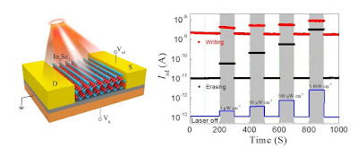
Light irradiation-controlled nonvolatile charge memory. Left: schematic of the memory device. Right: the optical-controlled writing and erasing process of source-drain current. (Courtesy: Q Li et al J. Phys. D: Appl. Phys. 10.1088/1361-6463/ab5737)


Topics: Applied Physics, Device Physics, Electrical Engineering, Materials Science, Nanotechnology


Qinliang Li, Cailei Yuan and Ting Yu from Jiangxi Normal University, along with Qisheng Wang and Jingbo Li from South China Normal University, are developing nonvolatile charge memory devices with simple structures. Wang explains how the optically controllable devices combine the functions of light sensing and electrical storage.

The research is reported in full in Journal of Physics D: Applied Physics, published by IOP Publishing – which also publishes Physics World.

What was the motivation for the research and what problem were you trying to solve?


Nonvolatile memory devices are central to modern communication and information technology. Among various material systems, emerging two dimensional (2D) materials offer a promising platform for next-generation data-storage devices due to their unique planar structure and brilliant electronic properties. However, 2D materials-based nonvolatile memory devices have complicated architectures with multilayer stacking of 2D materials, metals, organics or oxides. This limits the capacity for device miniaturization, scalability and integration functionality.


In this work, we are trying to design a nonvolatile charge memory with simple device architecture. We also expect to explore a new type of optical control on the charge storage devices, which may bring us smart operation on data deposition and communication.


Nonvolatile charge memory device shows excellent room-temperature performance, Physics World
Qisheng Wang is professor at the Institute of Semiconductor Science and Technology, South China Normal University

Read more…

Electron River...

electron_river_no_foam300.jpg
A river made of graphene with the electrons flowing like water.
Courtesy: Ryan Allen and Peter Allen, Second Bay Studios


Topics: Electron Configuration, Graphene, Nanotechnology


Electrons can behave like a viscous liquid as they travel through a conducting material, producing a spatial pattern that resembles water flowing through a pipe. So say researchers in Israel and the UK who have succeeded in imaging this hydrodynamic flow pattern for the first time using a novel scanning probe technique. The result will aid developers of future electronic devices, especially those based on 2D materials like graphene in which electron hydrodynamics is important.

We are all familiar with the distinctive patterns formed by water flowing in a river or stream. When the water encounters an obstacle – such as the river bank or a boat – the patterns change. The same should hold true for electron flow in a solid if the interactions between electrons are strong. This rarely occurs under normal conditions, however, since electrons tend to collide with defects and impurities in the material they travel through, rather than with each other.

Making electrons hydrodynamic

Conversely, if a material is made very clean and cooled to low temperatures, it follows that electrons should travel across it unperturbed until they collide with its edges and walls. The resulting ballistic transport allows electrons to flow with a uniform current distribution because they move at the same rate near the walls as at the center of the material.

If the temperature of this material is then increased, the electrons can begin to interact. In principle, they will then scatter off each other more frequently than they collide with the walls. In this highly interacting, hydrodynamic regime, the electrons should flow faster near the center of a channel and slower near its walls – the same way that water behaves when it flows through a pipe.


Electrons flow like water in ultra-pure graphene, Belle Dumé, Physics World

Read more…

The Next FET...

CNTFET.png
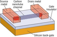
Source: Modeling Carbon Nanotube FET Physics in COMSOL Multiphysics®
 

Topics: Applied Physics, Carbon Nanotubes, Field Effect Transistors, Nanotechnology


Silicon field-effect transistors (FETs) were developed in the late 1950s as a scaled-down, energy-efficient substitute for bipolar junction transistors. They paved the way for the high-density integrated circuits that today underlie most electronics (see the article by Alan Fowler, Physics Today, October 1993, page 59). With their lower gate voltages, carbon nanotube FETs could surpass silicon FET energy efficiency by nearly a factor of 10. In 2013 Subhasish Mitra, Max Shulaker (then at Stanford University), and coworkers made the first CNFET microprocessor; it comprised 178 transistors and could run a single operation.

Variability caused by the production process has made moving beyond that proof-of-concept computer challenging. Gage Hills, Christian Lau, and coworkers in Shulaker’s group at MIT have now overcome that hurdle with a protocol for wafer-scale CNFET microprocessor production. Their technique is also compatible with existing CMOS infrastructure, which lowers the bar for future commercial implementation.

To remove carbon nanotube aggregates—a common contaminant from CNT deposition on silicon wafers—the researchers spin-coated a layer of adhesive polymer over the device and then removed the aggregates using ultrasonic vibrations. In previous attempts, sonication damaged the nonaggregated CNTs. Using the photoresist binds them to the wafer, which preserves their function while removing more than 99% of the aggregates.


Production of carbon nanotube microprocessors gets scaled up
Christine Middleton, Physics Today

Read more…

2D MXenes...

solar-farm-662095604-iStock_Milos-Muller.jpg
Helper two-dimensional metal-carbide layers could improve perovskite solar cell stability and help make these complex solar cells a viable green energy option. Credit: iStock Milos-Muller


Topics: Condensed Matter Physics, Green Tech, Materials Science, Metamaterials, Nanotechnology, Solar Power


With the reality of climate change looming, the importance of realistic green energy sources is higher than ever. Solar cells are one promising avenue, as they can convert readily available visible and ultraviolet energy into usable electricity. In particular, perovskite materials sandwiched between other support layers have demonstrated impressive power conversion efficiencies. Current challenges reside in optimizing perovskite/support layer interfaces, which can directly impact power conversion and cell degradation. Researchers Antonio Agresti et al. under the direction of Aldo Di Carlo at the University of Rome Tor Vergata in Italy have investigated how cells containing two-dimensional titanium-carbide MXene support layers could improve perovskite solar cell performance.

To obtain good power conversion within a perovskite solar cell, all layers and layer interfaces within the cell must have good compatibility. Typical cells contain the active perovskite material sandwiched between two charge transport layers, which are then adjacent to their corresponding electrodes. Support layers may also be added. Charge mobility, energy barriers, interface energy alignment, and interfacial vacancies all impact compatibility and subsequent cell performance and stability. Thus, engineering well-suited interfaces with the cell is paramount to cell success and long-term stability, an important criterion for potential commercialization.

Two-dimensional buffer materials could help to modify and promote useful interface interactions. MXenes, a growing class of two-dimensional transitional metal carbides, nitrides, and carbonitrides, have shown impressive electronic properties that are easily tuned via surface modification. For example, the band gap of an MXene can be modified by changing the surface termination group from an oxygen atom to a hydroxide molecule. Additionally, MXene composition impacts the overall material performance. This type of fine-tuning allows impressive control over MXene properties and makes them ideal for interface adjustments.


Two-dimensional MXenes improve perovskite solar cell efficiency
Amanda Carr, Physics World

#P4TC: MXenes...August 24, 2015

Read more…

Boiling Superconductivity...

Hydride.png
Under pressure: calculated structure of lithium magnesium hydride. Lithium atoms appear in green, magnesium in blue and hydrogen in red. (Courtesy: Ying Sun et al/Phys. Rev. Lett.)


Topics: Chemistry, Materials Science, Nanotechnology, Superconductors


A material that remains a superconductor when heated to the boiling point of water has been predicted by physicists in China. Hanyu Liu, Yanming Ma and colleagues at Jilin University have calculated that lithium magnesium hydride will superconduct at temperatures as high as 473 K (200 °C).

The catch is that the hydrogen-rich material must be crushed at 250 GPa, which is on par with pressures at the center of the Earth. While such a pressure could be achieved in the lab, it would be very difficult to perform an experiment to verify the prediction. The team’s research could, however, lead to the discovery of more practical high-temperature superconductors.

Superconductors are materials that, when cooled below a critical temperature, will conduct electricity with zero resistance. Most superconductors need to be chilled to very low temperatures, so the holy grail of superconductivity research is to find a substance that will superconduct at room temperature. This would result in lossless electricity transmission and boost technologies that rely on the generation or detection of magnetic fields.


Superconductivity at the boiling temperature of water is possible, say physicists
Hamish Johnston, Physics World

Read more…

Nanocones...

Nanocones.jpg
A carbon nanocone includes nitrogen atoms around the periphery to improve the material’s solubility. Carbon atoms are shown in gray; hydrogen in white; nitrogen in blue; and oxygen in red.


Topics: Applied Physics, Chemistry, Graphene, Nanotechnology


Graphene, buckyballs, and carbon nanotubes now have a new family member, the nanocone, adding to the types of all-carbon nanostructures with remarkable electronic and optical characteristics and bringing its own promising properties. (J. Am. Chem. Soc., 2019, DOI: 10.1021/jacs.9b06617) Such molecules could be useful for developing efficient organic solar cells or as sensor molecules.

Organic chemist Frank Würthner and postdoctoral researcher Kazutaka Shoyama of the University of Würzburg came up with the method for synthesizing the nanocones, which are 1.68 nm in diameter and 0.432 nm tall. A five-atom ring of carbons forms the cone’s tip. The team used a cross-coupling annulation cascade to add hexagons around the edges of the ring until the molecule grew to 80 carbons. The team added five nitrogen atoms around the periphery of the cone, increasing the crystal’s solubility.


Nanocones extend the graphene toolbox, Neil Savage, Chemical & Engineering News

Read more…

Decoding Sweat...

wrist.jpg
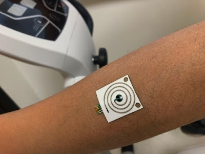
New wearable sensors developed by scientists at UC Berkeley can provide real-time measurements of sweat rate and electrolytes and metabolites in sweat. (Credit: Bizen Maskey, Sunchon National University)


Topics: Biophysics, Biotechnology, Microfluidics, Nanotechnology, Research


A new scalable, high-throughput fabrication process that makes use of roll-to-roll printing and laser cutting can produce wearable sweat sensors rapidly and reliably and on a large scale. The devices, which can almost instantly detect and analyse electrolytes, metabolites and other biomolecules contained in sweat, could be employed in real-world applications and not just as laboratory prototypes.

Analyzing sweat is a non-invasive way to monitor a range of biomolecules, from small electrolytes to metabolites and hormones and larger proteins that come from deeper in the body. Indeed, sweat sensing has already been used to medically diagnose diseases like cystic fibrosis and autonomic neuropathy and to assess fluid and electrolyte balance in endurance athletes.

Traditional sweat sensors collect sweat from the body at different times and then analyse it. This means that the devices can’t be used to detect real-time changes in sweat composition – during physical activity, for example, or to monitor glucose levels in diabetic patients. Wearable sensors, which make use of flexible and hybrid electronics, overcome this problem by allowing for in-situ sweat measurements with real-time feedback. However, it is still difficult to reliably make sweat sensor components (including microfluidic chip and sensing electrodes) in large quantities and with good reproducibility.


Wearable patches could ‘decode’ sweat, Belle Dumé, Physics World

Read more…

Lamina Tenuissima...

thinnest-optical-device-2.jpg
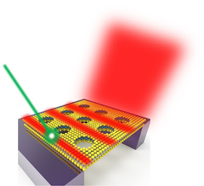
Illustration of a tungsten disulfide monolayer suspended in air and patterned with a square array of nanoholes. Upon laser excitation, the monolayer emits photoluminescence. A portion of this light couples into the monolayer and is guided along the material. At the nanohole array, periodic modulation in the refractive index causes a small portion of the light to decay out of the plane of the material, allowing the light to be observed as guided mode resonance. Courtesy: E Cubukcu, UCSD


Note: lamina tenuissima = thinnest (Latin)

Topics: Applied Physics, Nanotechnology, Optical Physics, Photonics


Researchers have succeeded in making the thinnest ever optical device in the form of a waveguide just three atomic layers thick. The device could lead to the development of higher density optoelectronic chips.

Optical waveguides are crucial components in data communication technologies but scaling them down to the nanoscale has proved to be no easy task, despite important advances in nano-optics and nanomaterials. Indeed, the thinnest waveguide used in commercial applications today is hundreds of nanometres thick and researchers are studying nanowire waveguides down to 50 nm in the laboratory.

“We have now pushed this limit down to just three atoms thick,” says Ertugrul Cubukcu of the University of California at San Diego, who led this new research effort. “Such a thin waveguide, which is at the ultimate limit for how thin an optical waveguide can be built, might potentially lead to a higher density of waveguides or optical elements on an optoelectronic chip – in the same way that ever smaller transistors have led to a higher density of these devices on an electronic chip.”

Cubukcu and colleagues’ waveguide is just six angstroms thick. This makes it 104 times thinner than a typical optical fiber and about 500 times thinner than on-chip optical waveguides in integrated photonic circuits.


Three-atom-thick optical waveguide is the thinnest ever, Belle Dumé, Physics World

Read more…

Cyclocarbon...

5d568358294db.jpg
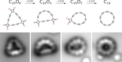
From left to right, precursor molecule C24O6, intermediates C22O4 and C20O2 and the final product cyclo [18]carbon C18 created on surface by dissociating CO masking groups using atom manipulation. The bottom row shows atomic force microscopy (AFM) data using a CO functionalized tip. Credit: IBM Research


Topics: Applied Physics, Atomic Force Microscopy, Chemistry, Nanotechnology, Research


A team of researchers from Oxford University and IBM Research has for the first time successfully synthesized the ring-shaped multi-carbon compound cyclocarbon. In their paper published in the journal Science, the group describes the process they used and what they learned about the bonds that hold a cyclocarbon together.

Carbon is one of the most abundant elements, and has been found to exist in many forms, including diamonds and graphene. The researchers with this new effort note that much research has been conducted into the more familiar forms (allotropes) how they are bonded. They further note that less well-known types of carbon have not received nearly as much attention. One of these, called cyclocarbon, has even been the topic of debate. Are the two-neighbor forms bonded by the same length bonds, or are there alternating bonds of shorter and longer lengths? The answer to this question has been difficult to find due to the high reactivity of such forms. The researchers with this new effort set themselves the task of finding the answer once and for all.

The team's approach involved creating a precursor molecule and then whittling it down to the desired form. To that end, they used atomic force microscopy to create linear lines of carbon atoms atop a copper substrate that was covered with salt to prevent the carbon atoms from bonding with the subsurface. They then joined the lines of atoms to form the carbon oxide precursor C24O6, a triangle-shaped form. Next, the team applied high voltage through the AFM to shear off one of the corners of the triangle, resulting in a C22O4 form. They then did the same with the other two corners. The result was a C18 ring—an 18-atom cyclocarbon. After creating the ring, the researchers found that the bonds holding it together were the alternating long- and short-type bonds that had been previously suggested.


Ring-shaped multi-carbon compound cyclocarbon synthesized, Bob Yirka , Phys.org

Read more…

Smart Packaging...

PWNANOApr18-pragmatIC-wafer-image.jpg
Cheaper flexible integrated circuits open up new markets. (Courtesy: PragmatIC)


Topics: Applied Physics, Moore's Law, Semiconductor Technology, Nanotechnology


For more than 50 years, progress in the electronics industry has been guided by Moore’s law: the idea that the number of transistors in a silicon-based integrated circuit (IC) will double approximately every 18 months. The consequences of this doubling include a continual reduction in the size of silicon ICs, as it becomes possible to provide increasingly complex and high-performance functionality in smaller and smaller areas of silicon, and at progressively lower cost relative to the circuits’ processing power.

Moore’s law is an empirical rule of thumb rather than a robust physical principle, and much has been written about how, why and when it will eventually fail. But even before we reach that point, manufacturers are already finding that, in practice, the cost savings associated with reducing the size, or “footprint”, of ICs will only carry them so far. The reason is that below a certain minimum size, ICs become difficult to handle easily or effectively. For highly complex circuitry, such as that found in computers with many millions of transistors in a single IC, this limit on handling size may not be a consideration. However, for applications that require less complex circuits, the size constraint imposed by the physical aspect of handling ICs becomes a limiting factor in their cost.

The approach we have taken at PragmatIC is to use thin, flexible substrates, rather than rigid silicon, as the base for building our circuits. The low cost of the materials involved and the relatively low complexity of our target applications alters the economics around circuit footprint and overall IC cost. Accepting a larger footprint can lower capital expenditure because it means that ultrahigh-end precision tooling is not required to fabricate our circuits during the manufacturing process. In turn, for low-complexity applications, this can lead to a lower final IC cost.

The resulting flexible integrated circuits, or FlexICs, are thinner than a human hair, so they can easily be embedded in everyday objects. They also cost around 10 times less than silicon ICs, making it economically viable for them to appear in trillions of smart objects that engage with consumers and their environments. Since the technology was developed, PragmatIC FlexICs have been trialed in a wide variety of markets, including consumer goods, games, retail, and the pharmaceutical and security sectors.


A smart approach to smart packaging
Catherine Ramsdale is vice-president of device development at PragmatIC

Read more…