 |
| Source: Link Below |
(Nanowerk Spotlight) The difficulties associated with precisely manipulating nanomaterials to turn nanoscale structures into reliable functional devices – at a reasonable cost – is one of the key challenges that needs to be overcome in mass-manufacturing nanodevices (other than computer chips, which require massive amounts of capital investment).
One of the most restricting parameters in nanofabrication is the difficulty involved with controllably patterning materials at precise locations in a repeatable manner over relatively large areas. The traditional process of randomly placing nanomaterials on a substrate typically leads to highly variable performance of the resultant functionalized devices.
Conventional lithography methods that are used in computer chip manufacturing are not only very expensive and wasteful, they also are reaching physical limitations. To overcome these issues, researchers have been developing a range of alternative, resist-free nanopatterning techniques, among them dip pen nanolithography, oxidation nanolithography, or colloidal self-assembly (see: "3D nanolithography without the expensive hardware").
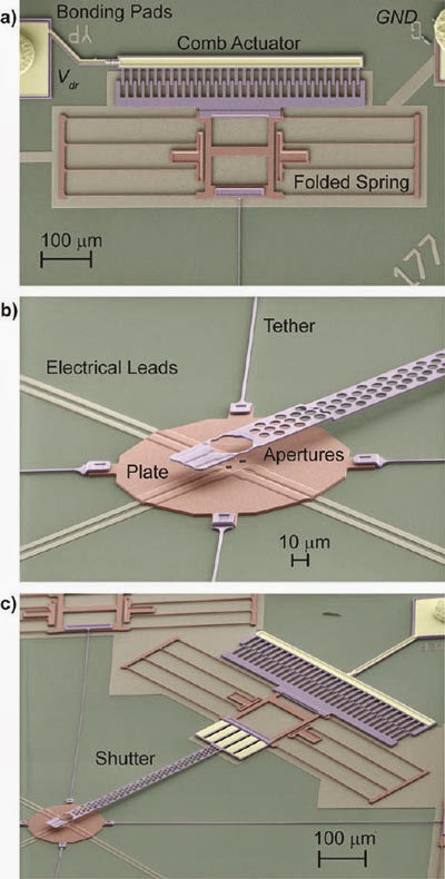
A novel microelectromechanical system (MEMS)-based mask writer has now been developed by a team of researchers at Boston University. The device allows to directly write structures at the nanoscale without the need to use photoresist, lift-off techniques or other complex and expensive approaches. The technique uses a MEMS plate with apertures drilled into it and a shutter so that one can, in effect, spray paint with atoms. With the shutter, the process can be turned on and off.
Nanowerk.com:
Atomic calligraphy - using MEMS to write nanoscale structures
NIST: Building a Fab on a Chip, David Bishop
Comments