 |
| Source: Link for Technology Review follows |
TECHNOLOGY REVIEW: A new technique for creating pipes and tunnels deep inside silicon chips could change the way engineers make microfluidic machines and optoelectronic devices.
One of the enabling technologies of the modern world is the ability to construct ever smaller devices out of silicon. At first, these devices were purely electronic—diodes, transistors, capacitors and the like. But more recently, engineers have carved light pipes, fluid-pumping networks, and entire chemistry laboratories out of silicon.
The technique that makes all this possible is photolithography, which allows engineers to build on or etch the surface of silicon in very precise patterns. The devices—whether electronic, fluidic, or optical—are built up layer by layer. Everything is done in two dimensions on the surface of silicon and then added together to create 3-D shapes.
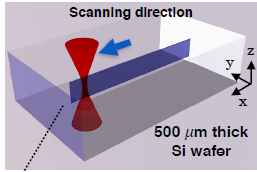
But what if it were possible to carve out structures beneath the surface of silicon, to create 3-D caves of almost any shape? Today, Onur Tokel at Bilkent University in Turkey and a few pals say they have developed just such a technique that can create networks of pipes and tunnels beneath the surface without any discernable change to the silicon surface.
The new technique relies on the fact that silicon is transparent to infrared light, which passes through silicon like sunlight through glass, at least at low intensities. When the light gets stronger, it can interact with electrons inside the material, generating currents and shaking the very crystal structure of the material. These effects are hard to predict and control but Tokel and co have found a way to use them to their advantage.
Abstract
Micromachining of silicon with lasers is being investigated since the 1970s. So far generating subsurface modifications buried inside the bulk of the silicon without damaging the surface has not resulted in success. Here, we report a method for photo-inducing buried structures in doped silicon wafers with pulsed infrared lasers without modifying the wafer surface. We demonstrate large aspect-ratio, continuous multilevel subsurface structures, with lengths on the millimetre scale, while having sub-micron widths. We further demonstrate spatial information encoding capabilities embedded in subsurface silicon barcodes based on an optical coherence tomography (OCT) readout. The demonstrated silicon processing technology can be used for the realization of multilayered silicon chips, optofluidics and on-chip quantum optics experiments.
Physics arXiv: Laser-Writing in Silicon for 3D Information Processing
O. Tokel, A. Turnali, I. Pavlov, S. Tozburun, I. Akca, F. O. Ilday
Comments