 |
| A. Houck/Princeton |
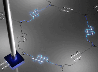
Figure 1: Scanning defect microscopy provides a map of photons in a resonator lattice. Houck and colleagues demonstrated the technique using 49 resonators (grey lines) that were coupled together to form a kagome lattice. This configuration consists of a triangular arrangement of three resonators at each point in a honeycomb lattice.
Topics: Electrical Engineering, Nanotechnology, Quantum Electrodynamics
A scanning probe detects the quantum states of photons in a microwave circuit, providing the information needed for quantum simulations.
Quantum mechanics rules the dynamics of light and matter. Yet performing a quantum-mechanical simulation of a material from first principles is practically impossible on a classical computer because the complexity of the simulation increases exponentially with the number of particles involved. The solution, according to Richard Feynman, was to build a machine out of quantum building blocks that could directly emulate the material itself [1]. Prototypes of such quantum simulators that are based on ultracold atoms, ions, photons, and superconducting microwave circuits are now available [2], with the latter, in particular, having attracted Silicon Valley’s interest. The challenge with these circuit-based simulators, however, is that they are 2D, which complicates the readout of their constituent elements. Andrew Houck from Princeton University, New Jersey, and colleagues have now delivered an attractive solution by developing a technique [3], called scanning defect microscopy (Fig. 1), that determines the number of photons occupying each mode of a 2D microwave circuit. It is this information that would serve as the fundamental input and output for certain quantum simulations.
Superconducting microwave circuits combine electronic and photonic degrees of freedom [4, 5]. The main element of the circuit is a transmission line, which is made up of a central superconducting wire separated by a gap from two grounded plates. All of these structures are on a single plane, as if one had taken a 2D slice through a coaxial cable. When truncated, the transmission line becomes a resonator, which can host discrete photon modes within its gaps. Large lattices of resonators can be engineered in various 1D or 2D geometries by coupling two, three, or more resonators together via a capacitive interface. In many ways, photons in such devices behave similarly to electrons in a solid.
To make microwave circuits that can simulate quantum phenomena faster than a classical computer, however, resonator lattices have to be integrated with superconducting qubits. Such qubits are controlled with electrical currents in a Josephson tunnel junction, and in many respects, they behave like artificial atoms, which couple to the photons in the circuit. As a result, superconducting microwave circuits can be used to explore the coupling between the quantum states of light and matter, the regime of circuit quantum electrodynamics (cQED). Photons in these devices often exhibit striking matter-like behavior [6, 7], providing the basis for the simulation of complex materials. Such circuits can be fabricated on a substrate using standard lithographic techniques, with qubits and resonators that are hundreds of micrometers or even millimeters in size.
APS Viewpoint: A Bird’s Eye View of Circuit Photons
Sebastian Schmidt, Institute for Theoretical Physics, ETH Zurich, 8093 Zurich, Switzerland
Comments