electrical_engineering (7)

Threshold Cryptography...

20ITL011_threshold.gif
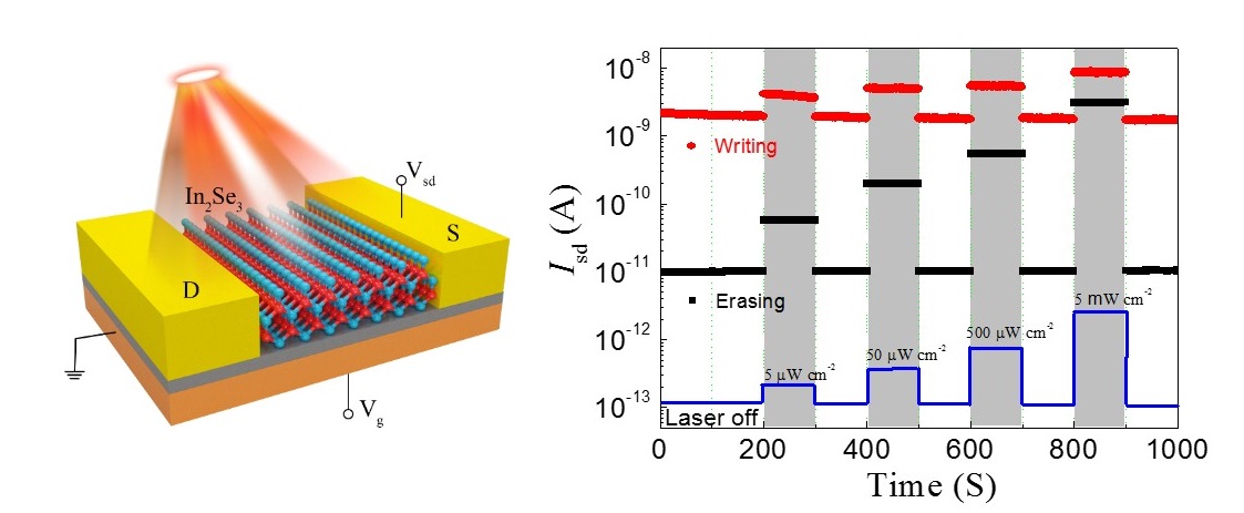
This artist’s conception of threshold cryptography shows a lock that can only be opened by three people working together. When the threshold cryptosystem receives a request to process information with a secret key, it initially splits the key into shares and sends them to the entire group, each share to a different participant. The three people must agree to work together and also perform their own secret operations on the incoming message. From these actions, each person uses their share key — represented by the three colored circles — to process the message, and then sends the result back to the system. Only the combination of all three partial results can open the lock, reducing the likelihood that a single corrupt party could compromise the system.


Topics: Cryptography, Computer Science, Electrical Engineering, NIST

A new publication by cryptography experts at the National Institute of Standards and Technology (NIST) proposes the direction the technical agency will take to develop a more secure approach to encryption. This approach, called threshold cryptography, could overcome some of the limitations of conventional methods for protecting sensitive transactions and data.

The document, released today in a final version as NIST Roadmap Toward Criteria for Threshold Schemes for Cryptographic Primitives (NISTIR 8214A), offers an outline for developing a new way to implement the cryptographic tools that developers use to secure their systems. Its authors are inviting the cryptography community to collaborate with them on NIST’s budding Threshold Cryptography project, which in part seeks to ensure that threshold implementations are interoperable.

“We are kicking the threshold cryptography development effort into high gear,” said Apostol Vassilev, a NIST computer scientist. “Over the coming months, the Threshold Cryptography project will be engaging with the public to define criteria for this work. We want to get feedback from the community so we can consider a variety of threshold schemes and standardization paths.”

Threshold cryptography takes its name from the idea that individual keyholders cannot open a lock on their own, as is common in conventional cryptography. Instead, out of a group of keyholders, there must be a minimum number of them — a “threshold” number — working together to open the lock. In practice, this lock is an electronic cryptosystem that protects confidential information, such as a bank account number or an authorization to transfer money from that account.

NIST Kick-Starts ‘Threshold Cryptography’ Development Effort

Read more…

So Much for Moore...

3nmpic1.png
Figure 1: Planar transistors vs finFETs vs nanosheet FET. Source: Samsung


Topics: Applied Physics, Electrical Engineering, Moore's Law, Nanotechnology, Semiconductor Technology


So much for the Moore's law limit. Although under current circumstances, the progression might be stalled by our current viral situation: the cost of chips will go higher, and consumers are currently making choices on food, jobs and toilet paper, not gadgets.

Select foundries are beginning to ramp up their new 5nm processes with 3nm in R&D. The big question is what comes after that.

Work is well underway for the 2nm node and beyond, but there are numerous challenges as well as some uncertainty on the horizon. There already are signs that the foundries have pushed out their 3nm production schedules by a few months due to various technical issues and the unforeseen pandemic outbreak, according to analysts. COVID-19 has slowed the momentum and impacted the sales in the IC industry.

This, in turn, is likely to push back the roadmaps beyond 3nm. Nevertheless, the current climate hasn’t stopped the semiconductor industry. Today, foundries and memory makers are running at relatively high fab utilization rates.

Behind the scenes, meanwhile, foundries and their customers continue to develop their 3nm and 2nm technologies, which are now slated for roughly 2022 and 2024, respectively. Work is also underway for 1nm and beyond, but that’s still far away.

Starting at 3nm, the industry hopes to make the transition from today’s finFET transistors to gate-all-around FETs. At 2nm and perhaps beyond, the industry is looking at current and new versions of gate-all-around transistors.

At these nodes, chipmakers will likely require new equipment, such as the next version of extreme ultraviolet (EUV) lithography. New deposition, etch and inspection/metrology technologies are also in the works.

Needless to say, the design and manufacturing costs are astronomical here. The design cost for a 3nm chip is $650 million, compared to $436.3 million for a 5nm device, and $222.3 million for 7nm, according to IBS. Beyond those nodes, it’s too early to say how much a chip will cost.


Making Chips At 3nm And Beyond
Mark Lapedus and Ed Sperling, Semiconductor Engineering

Read more…

Silicon Sees the Light...

Hamish-8-April-2020-silicon-light-emitters-crop.jpg
Silicon sees the light: Elham Fadaly (left) and Alain Dijkstra in their Eindhoven lab. (Courtesy: Sicco van Grieken/SURF)


Topics: Optics, Electrical Engineering, Nanotechnology, Research, Solar Power, Spectroscopy


A light-emitting silicon-based material with a direct bandgap has been created in the lab, fifty years after its electronic properties were first predicted. This feat was achieved by an international team led by Erik Bakkers at Eindhoven University of Technology in the Netherlands. They describe the new nanowire material as the “Holy Grail” of microelectronics. With further work, light-emitting silicon-based devices could be used to create low-cost components for optical communications, computing, solar energy and spectroscopy.

Silicon is the wonder material of electronics. It is cheap and plentiful and can be fabricated into ever smaller transistors that can be packed onto chips at increasing densities. But silicon has a fatal flaw when it comes to being used as a light source or solar cell. The semiconductor has an “indirect” electronic bandgap, which means that electronic transitions between the material’s valence and conduction bands involve vibrations in the crystal lattice. As a result, it is very unlikely that an excited electron in the conduction band of silicon will decay to the valence band by emitting light. Conversely, the absorption of light by silicon does not tend to excite valence electrons into the conduction band – a requirement of a solar cell.


Silicon-based light emitter is ‘Holy Grail’ of microelectronics, say researchers
Hamish Johnston, Physics World

Read more…

Moore's Reckoning...

UMC_14nm_finfet.png
Wiki Chip: 14 nm lithography process


Topics: Electrical Engineering, Moore's Law, Nanotechnology, Semiconductor Technology


It was hard to tell at the time — with the distraction of the Y2K bug, the explosion of reality television, and the popularity of post-grunge music — that the turn of the millennium was also the beginning of the end of easy computing improvements. A golden age of computing, which powered intensive data and computational science for decades, would soon be slowly drawing to a close. Even with novel ways of assembling computing systems, and new algorithms that take advantage of the architecture, the performance gains as predicted by Moore’s law were bound to come to an end — but in a way few people expected.

Moore’s law is the observation that the number of transistors in dense integrated circuits doubles roughly every two years. Before the turn of the millennium, all a computational scientist needed to do to have more than twice as fast a computer was to wait two years. Calculations that would have been impractical became accessible to desktop users. It was a time of plenty, and many problems could be solved by brute-force computing, from the quantum interactions of particles to the formation of galaxies. Giant lattices could be modeled, and enormous numbers of particles tracked. Improved computers enabled the analysis of genomic variations in entire communities and facilitated the advent of machine-learning techniques in AI.

Fundamental physics limits will ultimately put an end to transistor shrinkage in Moore’s law, and we are close to getting there. Today, chip production creates structures in silicon that are 14 nanometers wide and decreasing, and seven-nanometer elements are coming to market. At these sizes, thousands of these elements would fit in the width of a human hair. Feature sizes of less than five nanometers will probably be impossible because of quantum tunneling, in which electrons undesirably leak out of such narrow gaps.


A Reckoning for Moore’s Law
Why upgrading your computer every two years no longer makes sense.
Ian Fisk, Simon's Foundation

Read more…

Dr. Mark Dean, repost...

mark-dean.jpg
Dr. Mark Dean - Biography.com


Topics: African Americans, Computer Science, Electrical Engineering, Nanotechnology, STEM


This is admittedly a repost that appears during the month of February. The popular celebrities of sports, music and "reality" television dominate the imaginations of youth from all cultural backgrounds. It's important especially that African American children see themselves doing and making a living at STEM careers. A diverse workforce doesn't just "happen." Like the opposite of diversity - segregation - has to be intentionally planned and executed. For our country to survive and compete in nanotechnology, it MUST be a priority.

Computer scientist and engineer Mark Dean is credited with helping develop a number of landmark technologies, including the color PC monitor, the Industry Standard Architecture system bus and the first gigahertz chip.

Synopsis

Born in Jefferson City, Tennessee, in 1957, computer scientist and engineer Mark Dean helped develop a number of landmark technologies for IBM, including the color PC monitor and the first gigahertz chip. He holds three of the company's original nine patents. He also invented the Industry Standard Architecture system bus with engineer Dennis Moeller, allowing for computer plug-ins such as disk drives and printers.

Early Life and Education

Computer scientist and inventor Mark Dean was born on March 2, 1957, in Jefferson City, Tennessee. Dean is credited with helping to launch the personal computer age with work that made the machines more accessible and powerful.

From an early age, Dean showed a love for building things; as a young boy, Dean constructed a tractor from scratch with the help of his father, a supervisor at the Tennessee Valley Authority. Dean also excelled in many different areas, standing out as a gifted athlete and an extremely smart student who graduated with straight A's from Jefferson City High School. In 1979, he graduated at the top of his class at the University of Tennessee, where he studied engineering.

Innovation with IBM

Not long after college, Dean landed a job at IBM, a company he would become associated with for the duration of his career. As an engineer, Dean proved to be a rising star at the company. Working closely with a colleague, Dennis Moeller, Dean developed the new Industry Standard Architecture (ISA) systems bus, a new system that allowed peripheral devices like disk drives, printers and monitors to be plugged directly into computers. The end result was more efficiency and better integration.

But his groundbreaking work didn't stop there. Dean's research at IBM helped change the accessibility and power of the personal computer. His work led to the development of the color PC monitor and, in 1999, Dean led a team of engineers at IBM's Austin, Texas, lab to create the first gigahertz chip—a revolutionary piece of technology that is able to do a billion calculations a second.

In all, Dean holds three of the company's original nine patents for the IBM personal computer - a market the company helped create in 1981 and, in total, has more 20 patents associated with his name.


Biography.com: Mark Dean, Ph.D.

Read more…

Nonvolatile Charge Memory...

nonvolatile-charge-memory-device.jpg
Light irradiation-controlled nonvolatile charge memory. Left: schematic of the memory device. Right: the optical-controlled writing and erasing process of source-drain current. (Courtesy: Q Li et al J. Phys. D: Appl. Phys. 10.1088/1361-6463/ab5737)


Topics: Applied Physics, Device Physics, Electrical Engineering, Materials Science, Nanotechnology


Qinliang Li, Cailei Yuan and Ting Yu from Jiangxi Normal University, along with Qisheng Wang and Jingbo Li from South China Normal University, are developing nonvolatile charge memory devices with simple structures. Wang explains how the optically controllable devices combine the functions of light sensing and electrical storage.

The research is reported in full in Journal of Physics D: Applied Physics, published by IOP Publishing – which also publishes Physics World.

What was the motivation for the research and what problem were you trying to solve?


Nonvolatile memory devices are central to modern communication and information technology. Among various material systems, emerging two dimensional (2D) materials offer a promising platform for next-generation data-storage devices due to their unique planar structure and brilliant electronic properties. However, 2D materials-based nonvolatile memory devices have complicated architectures with multilayer stacking of 2D materials, metals, organics or oxides. This limits the capacity for device miniaturization, scalability and integration functionality.


In this work, we are trying to design a nonvolatile charge memory with simple device architecture. We also expect to explore a new type of optical control on the charge storage devices, which may bring us smart operation on data deposition and communication.


Nonvolatile charge memory device shows excellent room-temperature performance, Physics World
Qisheng Wang is professor at the Institute of Semiconductor Science and Technology, South China Normal University

Read more…

Structured Light...

 
structuredli.jpg
This image shows the creation of hybrid entangled photons by combining polarization with a "twisted" pattern that carries orbital angular momentum. Credit: Forbes and Nape


Topics: Electrical Engineering, Electromagnetic Radiation, Quantum Computing, Quantum Electrodynamics, Quantum Mechanics


Structured light is a fancy way to describe patterns or pictures of light, but deservedly so as it promises future communications that will be both faster and more secure.

Quantum mechanics has come a long way during the past 100 years but still has a long way to go. In AVS Quantum Science researchers from the University of Witwatersrand in South Africa review the progress being made in using structured light in quantum protocols to create a larger encoding alphabet, stronger security and better resistance to noise.

"What we really want is to do quantum mechanics with patterns of light," said author Andrew Forbes. "By this, we mean that light comes in a variety of patterns that can be made unique—like our faces."

Since patterns of light can be distinguished from each other, they can be used as a form of alphabet. "The cool thing is that there are, in principle at least, an infinite set of patterns, so an infinite alphabet is available," he said.

Traditionally, quantum protocols have been implemented with the polarization of light, which has only two values—a two-level system with a maximum information capacity per photon of just 1 bit. But by using patterns of light as the alphabet, the information capacity is much higher. Also, its security is stronger, and the robustness to noise (such as background light fluctuations) is improved.

"Patterns of light are a route to what we term high-dimensional states," Forbes said. "They're high dimensional, because many patterns are involved in the quantum process. Unfortunately, the toolkit to manage these patterns is still underdeveloped and requires a lot of work."
 

Structured light promises path to faster, more secure communications
American Institute of Physics, Phys.org

Read more…