optics (15)

Nano Racetracks...

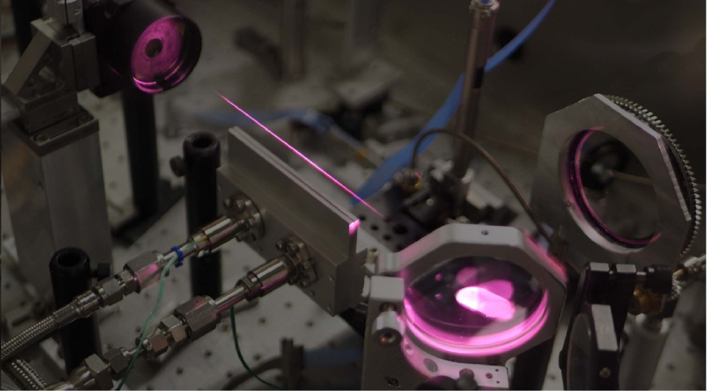
In this image, optical pulses (solitons) can be seen circling through conjoined optical tracks. (Image: Yuan, Bowers, Vahala, et al.) An animated gif is at the original link below.

Topics: Applied Physics, Astronomy, Electrical Engineering, Materials Science, Nanoengineering, Optics

(Nanowerk News) When we last checked in with Caltech's Kerry Vahala three years ago, his lab had recently reported the development of a new optical device called a turnkey frequency microcomb that has applications in digital communications, precision timekeeping, spectroscopy, and even astronomy.

This device, fabricated on a silicon wafer, takes input laser light of one frequency and converts it into an evenly spaced set of many distinct frequencies that form a train of pulses whose length can be as short as 100 femtoseconds (quadrillionths of a second). (The comb in the name comes from the frequencies being spaced like the teeth of a hair comb.)

Now Vahala, Caltech's Ted and Ginger Jenkins, Professor of Information Science and Technology and Applied Physics and executive officer for applied physics and materials science, along with members of his research group and the group of John Bowers at UC Santa Barbara, have made a breakthrough in the way the short pulses form in an important new material called ultra-low-loss silicon nitride (ULL nitride), a compound formed of silicon and nitrogen. The silicon nitride is prepared to be extremely pure and deposited in a thin film.

In principle, short-pulse microcomb devices made from this material would require very low power to operate. Unfortunately, short light pulses (called solitons) cannot be properly generated in this material because of a property called dispersion, which causes light or other electromagnetic waves to travel at different speeds, depending on their frequency. ULL has what is known as normal dispersion, and this prevents waveguides made of ULL nitride from supporting the short pulses necessary for microcomb operation.

In a paper appearing in Nature Photonics ("Soliton pulse pairs at multiple colors in normal dispersion microresonators"), the researchers discuss their development of the new micro comb, which overcomes the inherent optical limitations of ULL nitride by generating pulses in pairs. This is a significant development because ULL nitride is created with the same technology used for manufacturing computer chips. This kind of manufacturing technique means that these microcombs could one day be integrated into a wide variety of handheld devices similar in form to smartphones.

The most distinctive feature of an ordinary microcomb is a small optical loop that looks a bit like a tiny racetrack. During operation, the solitons automatically form and circulate around it.

"However, when this loop is made of ULL nitride, the dispersion destabilizes the soliton pulses," says co-author Zhiquan Yuan (MS '21), a graduate student in applied physics.

Imagine the loop as a racetrack with cars. If some cars travel faster and some travel slower, then they will spread out as they circle the track instead of staying as a tight pack. Similarly, the normal dispersion of ULL means light pulses spread out in the microcomb waveguides, and the microcomb ceases to work.

The solution devised by the team was to create multiple racetracks, pairing them up so they look a bit like a figure eight. In the middle of that '8,' the two tracks run parallel to each other with only a tiny gap between them.

Conjoined 'racetracks' make new optical devices possible, Nanowerk.

Read more…

Microlenses...

12313740872?profile=RESIZE_710x

Chromatic imaging of white light with a single lens (left) and achromatic imaging of white light with a hybrid lens (right). Credit: The Grainger College of Engineering at the University of Illinois Urbana-Champaign

Topics: 3D Printing, Additive Manufacturing, Applied Physics, Materials Science, Optics

Using 3D printing and porous silicon, researchers at the University of Illinois Urbana-Champaign have developed compact, visible wavelength achromats that are essential for miniaturized and lightweight optics. These high-performance hybrid micro-optics achieve high focusing efficiencies while minimizing volume and thickness. Further, these microlenses can be constructed into arrays to form larger area images for achromatic light-field images and displays.

This study was led by materials science and engineering professors Paul Braun and David Cahill, electrical and computer engineering professor Lynford Goddard, and former graduate student Corey Richards. The results of this research were published in Nature Communications.

"We developed a way to create structures exhibiting the functionalities of classical compound optics but in highly miniaturized thin film via non-traditional fabrication approaches," says Braun.

In many imaging applications, multiple wavelengths of light are present, e.g., white light. If a single lens is used to focus this light, different wavelengths focus at different points, resulting in a color-blurred image. To solve this problem, multiple lenses are stacked together to form an achromatic lens. "In white light imaging, if you use a single lens, you have considerable dispersion, and so each constituent color is focused at a different position. With an achromatic lens, however, all the colors focus at the same point," says Braun.

The challenge, however, is that the required stack of lens elements required to make an achromatic lens is relatively thick, which can make a classical achromatic lens unsuitable for newer, scaled-down technological platforms, such as ultracompact visible wavelength cameras, portable microscopes, and even wearable devices.

A new (micro) lens on optics: Researchers develop hybrid achromats with high focusing efficiencies,  Amber Rose, University of Illinois Grainger College of Engineering

Read more…

Slits in Time...

11020504672?profile=RESIZE_584x

The classic double-slit experiment leads to characteristic interference patterns. Credit: Russell Knightly/SPL

Topics: Modern Physics, Optics, Quantum Mechanics

A celebrated experiment in 1801 showed that light passing through two thin slits interferes with itself, forming a characteristic striped pattern on the wall behind. Now, physicists have shown that a similar effect can arise with two slits in time rather than space: a single mirror that rapidly turns on and off causes interference in a laser pulse, making it change color.

The result is reported on 3 April in Nature Physics1. It adds a new twist to the classic double-slit experiment performed by physicist Thomas Young, which demonstrated the wavelike aspect of light, but also — in its many later reincarnations — that quantum objects ranging from photons to molecules have a dual nature of both particle and wave.

The rapid switching of the mirror — possibly taking just one femtosecond (one-quadrillionth of a second) — shows that certain materials can change their optical properties much faster than previously thought possible, says Andrea Alù, a physicist at the City University of New York. This could open new paths for building devices that handle information using light rather than electronic impulses.

Romain Tirole, a quantum physicist at Imperial College London, and his collaborators shot an infrared laser at a surface made of layers of gold and glass with a thin coating of indium tin oxide (ITO), a material common in smartphone screens.

Under normal conditions, ITO is transparent to infrared light. But the researchers were able to make the material reflective using a second laser, which excited electrons in the material, affecting its optical properties. This could be done with pulses from the second laser that lasted for around 200 femtoseconds.

The researchers positioned a light sensor along the reflected beam. When they shot two ultrashort pulses separated by a few tens of femtoseconds — therefore turning the ITO mirror on twice in rapid succession — they saw that the waveform of the twice-reflected light changed in response. It went from a simple, monochromatic wave to a more complex one.

The results also showed that the ITO took less than ten femtoseconds to get excited — much faster than expected theoretically or from previous measurements. “The reason why everybody else thought it would be slower is that they used a different technique to measure the response time, which was limited to 50–100 fs,” says co-author Riccardo Sapienza, a physicist at Imperial College.

Light waves squeezed through ‘slits in time,’ Davide Castelvecchi, Nature

Read more…

10998141656?profile=RESIZE_710x

Atomic analog: when a beam of light is shone into a water droplet, the light is trapped inside. (Courtesy: Javier Tello Marmolejo)

Topics: Modern Physics, Optics, Quantum Mechanics, Quantum Optics, Research

Light waves confined in an evaporating water droplet provide a useful model of the quantum behavior of atoms, researchers in Sweden and Mexico have discovered. Through a simple experiment, a team led by Javier Marmolejo at the University of Gothenburg has shown how the resonance of light inside droplets of specific sizes can provide robust analogies to atomic energy levels and quantum tunneling.

When light is scattered by a liquid droplet many times larger than its wavelength, some of the light may reflect around the droplet’s internal edge. If the droplet’s circumference is a perfect multiple of the light’s wavelength inside the liquid, the resulting resonance will cause the droplet to flash brightly. This is an optical example of a whispering gallery mode, whereby sound can reflect around a circular room.

This effect was first described mathematically by the German physicist Gustav Mie in 1908 – yet despite the simplicity of the scenario, the rich array of overlapping resonances it produces can create some incredibly complex patterns, some of which have yet to be studied in detail.

Optical Tweezers

To explore the effect in more detail, Marmolejo and the team devised an experiment where they confined water droplets using optical tweezers. They evaporated the liquid by heating it with a fixed-frequency laser. As the droplets shrank, their circumferences will sometimes equal a multiple of the laser’s wavelength. At these “Mie resonances,” the droplets flashed brightly.

As they studied this effect, the researchers realized that the flashing droplets are analogous to the quantum behaviors of atoms. In these “optical atoms,” orbiting electrons are replaced with resonating photons. The electrostatic potential that binds electrons to the nucleus is replaced by the droplet’s refractive index, which tends to trap light in the droplet by internal reflection. The quantized energy levels of an atom are represented by the droplet sizes where Mie resonances occur.

Flashing droplets could shed light on atomic physics and quantum tunneling, Sam Jarman, Physics World.

Read more…

Mirror, Mirror...

10780308878?profile=RESIZE_584x

Various views of a 3D-printed object are captured by a single camera using a dome-shaped array of mirrors. Left: The raw image. Right: closeups of some of the individual views. (Image: Sanha Cheong, SLAC National Accelerator Laboratory)

Topics: Applied Physics, Atomic-Scale Microscopy, Materials Science, Optics

(Nanowerk News) When it goes online, the MAGIS-100 experiment at the Fermi National Accelerator Laboratory and its successors will explore the nature of gravitational waves and search for certain kinds of wavelike dark matter. But first, researchers need to figure out something pretty basic: how to get good photographs of the clouds of atoms at the heart of their experiment.

Researchers at the Department of Energy's SLAC National Accelerator Laboratory realized that task would be perhaps the ultimate exercise in ultra-low light photography.

But a SLAC team that included Stanford graduate students Sanha Cheong and Murtaza Safdari, SLAC Professor Ariel Schwartzman, and SLAC scientists Michael Kagan, Sean Gasiorowski, Maxime Vandegar, and Joseph Frish found a simple way to do it: mirrors. By arranging mirrors in a dome-like configuration around an object, they can reflect more light towards the camera and image multiple sides of an object simultaneously.

And, the team reports in the Journal of Instrumentation ("Novel light field imaging device with an enhanced light collection for cold atom clouds"), that there's an additional benefit. Because the camera now gathers views of an object taken from many different angles, the system is an example of “light-field imaging”, which captures not just the intensity of light but also which direction light rays travel. As a result, the mirror system can help researchers build a three-dimensional model of an object, such as an atom cloud.

How do you take a better image of atom clouds? Mirrors - lots of mirrors, SLAC National Accelerator Laboratory

Read more…

Scrofulous Signaling...

9243654887?profile=RESIZE_584x

FIG. 1. Schematics of pulse sequences for spin-locking measurement with (a) two π/2 pulses and (b) two composite pulses. (c) Schematics of a SCROFULOUS composite pulse composed of three pulses. (d) Evolution of the spin state in the Bloch sphere. The spin state is initialized to the |0⟩ state by the first laser pulse. (e) The first π/2 pulse rotates the spin by 90∘ to the (−y)-direction. A y-driving microwave field is applied parallel to the spin in the rotation frame. (f) The second π/2 pulse rotates the spin by 90∘ to the (−z)-direction in the pulse sequence pattern A, or (g) the second −π/2 pulse rotates the spin by −90∘ to the z-direction in the pulse sequence pattern B. Finally, the spin state is read out from the PL by applying the second laser pulse. (h) Schematics of the experimental setup.

Topics: Applied Physics, Electrical Engineering, Materials Science, Optics

We present results of near-field radio-frequency (RF) imaging at micrometer resolution using an ensemble of nitrogen-vacancy (NV) centers in diamond. The spatial resolution of RF imaging is set by the resolution of an optical microscope, which is markedly higher than the existing RF imaging methods. High sensitivity RF field detection is demonstrated through spin locking. SCROFULOUS composite pulse sequence is used for manipulation of the spins in the NV centers for reduced sensitivity to possible microwave pulse amplitude error in the field of view. We present procedures for acquiring an RF field image under spatially inhomogeneous microwave field distribution and demonstrate a near-field RF imaging of an RF field emitted from a photolithographically defined metal wire. The obtained RF field image indicates that the RF field intensity has maxima in the vicinity of the edges of the wire, in accord with a calculated result by a finite-difference time-domain method. Our method is expected to be applied in a broad variety of application areas, such as material characterizations, characterization of RF devices, and medical fields.</em>

Near-field radio-frequency imaging by spin-locking with a nitrogen-vacancy spin sensor, Shintaro Nomura1,a), Koki Kaida1, Hideyuki Watanabe2, and Satoshi Kashiwaya3, Journal of Applied Physics

Read more…

Nano Laser...

9096373252?profile=RESIZE_584x

In their experiments, the researchers used ultrathin crystals consisting of a single layer of atoms. These sheets were sandwiched between two layers of mirror-like materials. The whole structure acts as a cage for light and is called a microcavity.

Topics: Applied Physics, Bose-Einstein Condensate, Lasers, Nanotechnology, Optics

Physicists have taken a step towards realizing the smallest-ever solid-state laser by generating an exotic quantum state known as a Bose-Einstein condensate (BEC) in quasiparticles consisting of both matter and light. Although the effect has so far only been observed at ultracold temperatures in atomically thin crystals of molybdenum diselenide (MoSe2), it might also be produced at room temperature in other materials.

When particles are cooled down to temperatures just above absolute zero, they form a BEC – a state of matter in which all the particles occupy the same quantum state and act in unison, like a superfluid. A BEC made up of tens of thousands of particles behaves as if it were just one giant quantum particle.

An international team of researchers led by Carlos Anton-Solanas and Christian Schneider from the University of Oldenburg, GermanySven Höfling of the University of Würzburg, GermanySefaattin Tongay at Arizona State University, US; and Alexey Kavokin of Westlake University in China, has now generated a BEC from quasiparticles known as exciton-polaritons in atomically thin crystals. These quasiparticles form when excited electrons in solids couple strongly with photons.

“Devices that can control these novel light-matter states hold the promise of a technological leap in comparison with current electronic circuits,” explains Anton-Solanas, who is in the quantum materials group at Oldenburg’s Institute of Physics. “Such optoelectronic circuits, which operate using light instead of electric current, could be better and faster at processing information than today’s processors.”

Anton-Solanas, Schneider, and colleagues studied crystals of MoSe2 that were just a single atomic layer thick. MoSe2belongs to a family of materials known as transition-metal dichalcogenides (TMDCs). In their bulk form, these materials act as indirect band-gap semiconductors. Still, when scaled down to a monolayer thickness, they behave as direct band-gap semiconductors, capable of efficiently absorbing and emitting light.

In their experiments, the researchers assembled sheets of MoSe2 less than a nanometer thick and sandwiched them between alternating layers of silicon dioxide and titanium dioxide (SiO2/TiO2), which reflect light like a mirror. The resulting structure is known as a microcavity and acts as a cage for light. “It’s like trapping the light-emitting material in a room filled with mirrors and mirrors only,” Tongay tells Physics World. “The light gets reflected these mirrors and is absorbed by the material back and forth.”

Exotic quantum state could make smallest-ever laser, Isabelle Dumé, Physics World

Read more…

Transparency...

7994019487?profile=RESIZE_710x

Credit: Johannes Zirkelbach/Max Planck Institute for the Science of Light


Topics: Applied Physics, Nanotechnology, Optics


At the focus of a laser, a 100-nm-wide gold nanoparticle can block more than half the light. If additional particles are added, the amount of blocked light increases exponentially, as modeled by the Beer-Lambert law. But theorists predict that in the right set of circumstances, the addition of a molecule would, counterintuitively, decrease the light blocked—that is, make the nanoparticle partially transparent.


Vahid Sandoghdar of the Max Planck Institute for the Science of Light and his colleagues have now shown that predicted partial transparency for a near-field coupled dye molecule (red in image) and a plasmonic nanoparticle (gold). The phenomenon is a result of the interference between the light scattered from the two.


To achieve the required coupling, the dye molecule must be in a particular orientation and less than a wavelength away from the gold nanoparticle. Controlling those parameters is tricky, so Sandoghdar and his colleagues left them to chance. The researchers started with an array of nanoparticles and then coated it with a molten crystal doped with dibenzoterrylene (DBT) dye molecules. After the colorless crystal solidified, the result was a stochastic distribution of DBT molecules.


Their strong, distinctive fluorescence made the dye molecules easy to find optically. But the team members needed to verify that the molecule was near-field coupled to a nanoparticle. They identified a particle with two nearby DBT molecules and shined [a] tunable titanium: sapphire laser on it. The nanoparticle acts as an antenna, which enhances the molecules’ fluorescence. Relative to the other, one DBT molecule had telltale signatures of near-field interactions: enhanced and spectrally broadened fluorescence and a shorter excited-state lifetime—1.4 ns compared with the usual 8.1 ns.


Nanoparticle turns partially transparent, Heather Hill, Physics Today


Read more…

Plasma Guides and Lasers...

rn-lasers-guided.jpg?w=1024

Lasers are used to create an indestructible optical fiber out of plasma.

Credit: Intense Laser-Matter Interactions Lab, University of Maryland

Topics: Lasers, Optics, Plasma, Research, Star Trek, Star Wars

In science fiction, firing powerful lasers looks easy — the Death Star can just send destructive power hurtling through space as a tight beam. But in reality, once a powerful laser has been fired, care must be taken to ensure it doesn’t get spread too thin.

If you’ve ever pointed a flashlight at a wall, you’ve observed an example of the diffusion of light. The farther you are from the wall, the more the beam spreads, resulting in a larger and dimmer spot of light. Lasers generally expand much more slowly than the beams from flashlights, but the effect of diffusion is important when the laser travels a long way or must maintain a high intensity.

Whether your goal is to achieve galactic domination or, more realistically, to accelerate electrons to incredible speeds for physics research, you’ll want as tight and powerful a beam as possible to maximize the intensity.

In their experiments, researchers can use devices called waveguides, like the optical fibers that might be carrying the internet throughout your neighborhood, to transport lasers while keeping them contained to narrow beams.

Plasma guides maintain focus of lasers, National Science Foundation Public Affairs

Read more…

APS...

Topics: COVID-19, Materials Science, Optics, Photonics, Research

From chemistry to materials science to COVID-19 research, the APS is one of the most productive X-ray light sources in the world. An upgrade will make it a global leader among the next generation of light sources, opening new frontiers in science.

In the almost 25 years since the Advanced Photon Source (APS), a U.S. Department of Energy (DOE) Office of Science User Facility, first opened at DOE’s Argonne National Laboratory, it has played an essential role in some of the most pivotal discoveries and advancements in science.

More than 5,000 researchers from around the world conduct experiments at the APS every year, and their work has, among many other notable successes, paved the way for better renewable batteries; resulted in the development of numerous new drugs; and helped to make vehicles more efficient, infrastructure materials stronger and electronics more powerful.

Advanced Photon Source Upgrade will transform the world of scientific research, Brett Hansard, Argonne National Laboratory

Read more…

Photography of the Invisible...

Figure

Figure 1. Sarah Frances Whiting (1847–1927) using a fluoroscope to examine the bones in her hand in Wellesley College’s physics laboratory, circa 1896. On the table in front of her is a Crookes tube mounted on a stand and an induction coil to modulate the voltage. (Courtesy of Wellesley College.)

Topics: Applied Physics, Optics, Women in Science, X-rays

In February 1896 Sarah Frances Whiting, founder of the physics and astronomy departments at Wellesley College, conducted a series of x-ray experiments. She was working only a few weeks after the public announcement of Wilhelm Röntgen’s discovery of the rays, and she was not alone; amateur and professional scientists at colleges, universities, and medical centers across the US were attempting to replicate and extend Röntgen’s results. But Whiting (see figure 1), who enlisted the assistance of a Wellesley colleague and several students, was among the first to do so successfully. Even more importantly, Whiting was the first woman—and almost certainly the first person, male or female—to do so in an undergraduate laboratory. Her original glass plates from the experiments do not survive, but 15 photographs printed from them (see the opening image of one such photo above) were recently rediscovered in a campus building slated for demolition. They provide a vivid reminder of Whiting’s success.

The x-ray experiments were only one instance in which Whiting drew on her keen engagement with contemporary scientific advances to offer her students an experience available to few undergraduates at the time, and to almost no women. Throughout her long career, Whiting introduced thousands of women to physics and astronomy, both fields then associated almost entirely with men. Her pedagogical efforts led many of her female students to pursue their own careers in the sciences.

Sarah Frances Whiting and the “photography of the invisible”

John S. Cameron is an emeritus professor of biological sciences and Jacqueline Marie Musacchio is a professor of art history at Wellesley College in Massachusetts.

Read more…

Touchless Print Scanning...

20ITL009_fingerprint-scanner_nch.jpg
Credit: N. Hanacek/NIST NIST evaluated several commercially available contactless fingerprint scanning technologies in its May 2020 report.


Topics: NIST, Optics, Research

The National Institute of Standards and Technology (NIST) has evaluated several commercially available contactless fingerprint scanning technologies, allowing users to compare their performance to conventional devices that require physical contact between a person’s fingers and the scanner.

The results of the study, published today as NIST Interagency Report (NISTIR) 8307: Interoperability Assessment 2019: Contactless-to-Contact Fingerprint Capture, show that devices requiring physical contact remain superior to contactless technology at matching scanned prints to images in a database. However, when contactless devices scan multiple fingers on a hand, it improves their performance. Contactless devices that scanned multiple fingers also seldom made “false positive” errors that incorrectly matched one person’s print with another’s record.

The publication updates NIST’s July 2018 study on contactless capture and is intended to assist organizations that use fingerprint-scanning technology.

“The report summarizes the state of the art of contactless fingerprint scanning,” said John Libert, one of the report’s authors. “It can help anyone interested in adopting contactless technology to evaluate the cost in performance they might pay by switching to contactless fingerprint capture.”

NIST Study Measures Performance Accuracy of Contactless Fingerprinting Tech

Read more…

Silicon Sees the Light...

Hamish-8-April-2020-silicon-light-emitters-crop.jpg
Silicon sees the light: Elham Fadaly (left) and Alain Dijkstra in their Eindhoven lab. (Courtesy: Sicco van Grieken/SURF)


Topics: Optics, Electrical Engineering, Nanotechnology, Research, Solar Power, Spectroscopy


A light-emitting silicon-based material with a direct bandgap has been created in the lab, fifty years after its electronic properties were first predicted. This feat was achieved by an international team led by Erik Bakkers at Eindhoven University of Technology in the Netherlands. They describe the new nanowire material as the “Holy Grail” of microelectronics. With further work, light-emitting silicon-based devices could be used to create low-cost components for optical communications, computing, solar energy and spectroscopy.

Silicon is the wonder material of electronics. It is cheap and plentiful and can be fabricated into ever smaller transistors that can be packed onto chips at increasing densities. But silicon has a fatal flaw when it comes to being used as a light source or solar cell. The semiconductor has an “indirect” electronic bandgap, which means that electronic transitions between the material’s valence and conduction bands involve vibrations in the crystal lattice. As a result, it is very unlikely that an excited electron in the conduction band of silicon will decay to the valence band by emitting light. Conversely, the absorption of light by silicon does not tend to excite valence electrons into the conduction band – a requirement of a solar cell.


Silicon-based light emitter is ‘Holy Grail’ of microelectronics, say researchers
Hamish Johnston, Physics World

Read more…

Hologram Printer...

newprintercr.jpg
The new printer uses low-power continuous wave lasers to create holograms on a highly sensitive photomaterial developed by the researchers. Credit: C Yves GENTET


Topics: 3D Objects, 3D Printing, Applied Physics, Holograms, Optics, Research


Researchers have developed a new printer that produces digital 3-D holograms with an unprecedented level of detail and realistic color. The new printer could be used to make high-resolution color recreations of objects or scenes for museum displays, architectural models, fine art or advertisements that do not require glasses or special viewing aids.

"Our 15-year research project aimed to build a hologram printer with all the advantages of previous technologies while eliminating known drawbacks such as expensive lasers, slow printing speed, limited field of view and unsaturated colors," said research team leader Yves Gentet from Ultimate Holography in France. "We accomplished this by creating the CHIMERA printer, which uses low-cost commercial lasers and high-speed printing to produce holograms with high-quality color that spans a large dynamic range."


New printer creates extremely realistic colorful holograms, The Optical Society, Phys.org

Read more…

How We See the Small...

800px-AFM_used_cantilever_in_Scanning_Electron_Microscope_magnification_1000x.jpg
View of cantilever on an atomic force microscope (magnification 1000x).
Credit: SecretDisc GFDL, CC-BY-SA-3.0


Topics: Atomic Force Microscopy, Nanotechnology, Optics, Scanning Electron Microscope


Cell reproduction, disease detection and semiconductor optimization are just some of the areas of research that have exploited the atomic force microscope. First invented by Calvin Quate, Gerd Binnig and Christoph Gerber in the mid 1980s, atomic force microscopy (AFM) brought the atomic resolution recently achieved by the scanning tunnelling microscope to non-conducting samples, and helped to catalyse the avalanche of science and technology based on nanostructures that now permeates all aspects of modern life from smartphones to tennis rackets. On 6 July 2019 Calvin Quate died aged 95 at his home in Menlo Park, California.

Long before the development of AFM, Quate’s research had made waves in microscopy. 1978 had seen the announcement of the scanning acoustic microscope, which achieved the sensitivity of optical microscopy but probed samples so softly that it could image the interiors of living cells without damaging them. The technique uses high frequency sound waves in place of light, which penetrate deep into structures to image internal structures non-destructively. It is widely used in quality control of electronic component assembly among other applications such as printed circuit boards and medical products.
 

Advanced microscopy pioneer leaves broad ranging legacy
Anna Demming, Physics World

Read more…