photonics (4)

Organic Solar Cells...

11217774072?profile=RESIZE_584x

Prof. Li Gang invented a novel technique to achieve breakthrough efficiency with organic solar cells. Credit: Hong Kong Polytechnic University

Topics: Chemistry, Green Tech, Materials Science, Photonics, Research, Solar Power

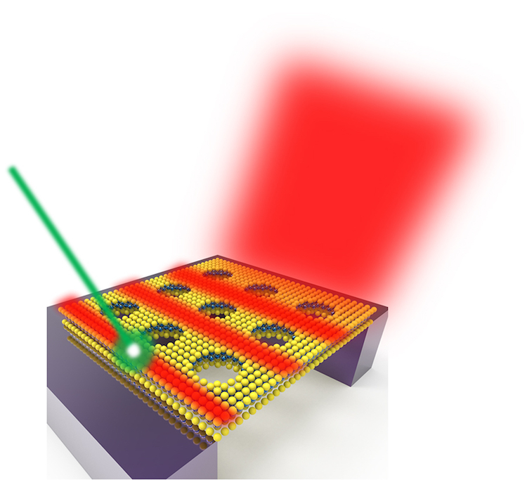
Researchers from The Hong Kong Polytechnic University (PolyU) have achieved a breakthrough power-conversion efficiency (PCE) of 19.31% with organic solar cells (OSCs), also known as polymer solar cells. This remarkable binary OSC efficiency will help enhance these advanced solar energy device applications.

The PCE, a measure of the power generated from a given solar irradiation, is considered a significant benchmark for the performance of photovoltaics (PVs), or solar panels, in power generation. The improved efficiency of more than 19% that was achieved by the PolyU researchers constitutes a record for binary OSCs, which have one donor and one acceptor in the photoactive layer.

Led by Prof. Li Gang, Chair Professor of Energy Conversion Technology, and Sir Sze-Yen Chung, Endowed Professor in Renewable Energy at PolyU, the research team invented a novel OSC morphology-regulating technique by using 1,3,5-trichlorobenzene as a crystallization regulator. This new technique boosts OSC efficiency and stability.

The team developed a non-monotonic intermediated state manipulation (ISM) strategy to manipulate the bulk-heterojunction (BHJ) OSC morphology and simultaneously optimize the crystallization dynamics and energy loss of non-fullerene OSCs. Unlike the strategy of using traditional solvent additives, which is based on excessive molecular aggregation in films, the ISM strategy promotes the formation of more ordered molecular stacking and favorable molecular aggregation. As a result, the PCE was considerably increased, and the undesirable non-radiative recombination loss was reduced. Notably, non-radiative recombination lowers the light generation efficiency and increases heat loss.

Researchers achieve a record 19.31% efficiency with organic solar cells. Hong Kong Polytechnic University. Tech Explore

Read more…

When Water Outpaces Silicon…

10948713060?profile=RESIZE_710x

On target: Water is fanned out through a specially developed nozzle, and then a laser pulse is passed through it to create a switch. (Courtesy: Adrian Buchmann)

Topics: Applied Physics, Lasers, Materials Science, Photonics, Semiconductor Technology

A laser-controlled water-based switch that operates twice as fast as existing semiconductor switches has been developed by a trio of physicists in Germany. Adrian Buchmann, Claudius Hoberg, and Fabio Novelli at Ruhr University Bochum used an ultrashort laser pulse to create a temporary metal-like state in a jet of liquid water. This altered the transmission of terahertz pulses over timescales of just tens of femtoseconds.

With the latest semiconductor-based switches approaching fundamental upper limits on how fast they can operate, researchers are searching for faster ways of switching signals. One unexpected place to look for inspiration is the curious behavior of water under extreme conditions – like those deep within ice-giant planets or created by powerful lasers.

Molecular dynamics simulations suggest water enters a metallic state at pressures of 300 GPa and temperatures of 7000 K. While such conditions do not occur on Earth, it is possible that this state contributes to the magnetic fields of Uranus and Neptune. To study this effect closer to home, recent experiments have used powerful, ultrashort laser pulses to trigger photo-ionization in water-based solutions – creating fleeting, metal-like states.

Water-based switch outpaces semiconductor devices, described in APL Photonics.

Read more…

APS...

Topics: COVID-19, Materials Science, Optics, Photonics, Research

From chemistry to materials science to COVID-19 research, the APS is one of the most productive X-ray light sources in the world. An upgrade will make it a global leader among the next generation of light sources, opening new frontiers in science.

In the almost 25 years since the Advanced Photon Source (APS), a U.S. Department of Energy (DOE) Office of Science User Facility, first opened at DOE’s Argonne National Laboratory, it has played an essential role in some of the most pivotal discoveries and advancements in science.

More than 5,000 researchers from around the world conduct experiments at the APS every year, and their work has, among many other notable successes, paved the way for better renewable batteries; resulted in the development of numerous new drugs; and helped to make vehicles more efficient, infrastructure materials stronger and electronics more powerful.

Advanced Photon Source Upgrade will transform the world of scientific research, Brett Hansard, Argonne National Laboratory

Read more…

Lamina Tenuissima...

thinnest-optical-device-2.jpg
Illustration of a tungsten disulfide monolayer suspended in air and patterned with a square array of nanoholes. Upon laser excitation, the monolayer emits photoluminescence. A portion of this light couples into the monolayer and is guided along the material. At the nanohole array, periodic modulation in the refractive index causes a small portion of the light to decay out of the plane of the material, allowing the light to be observed as guided mode resonance. Courtesy: E Cubukcu, UCSD


Note: lamina tenuissima = thinnest (Latin)

Topics: Applied Physics, Nanotechnology, Optical Physics, Photonics


Researchers have succeeded in making the thinnest ever optical device in the form of a waveguide just three atomic layers thick. The device could lead to the development of higher density optoelectronic chips.

Optical waveguides are crucial components in data communication technologies but scaling them down to the nanoscale has proved to be no easy task, despite important advances in nano-optics and nanomaterials. Indeed, the thinnest waveguide used in commercial applications today is hundreds of nanometres thick and researchers are studying nanowire waveguides down to 50 nm in the laboratory.

“We have now pushed this limit down to just three atoms thick,” says Ertugrul Cubukcu of the University of California at San Diego, who led this new research effort. “Such a thin waveguide, which is at the ultimate limit for how thin an optical waveguide can be built, might potentially lead to a higher density of waveguides or optical elements on an optoelectronic chip – in the same way that ever smaller transistors have led to a higher density of these devices on an electronic chip.”

Cubukcu and colleagues’ waveguide is just six angstroms thick. This makes it 104 times thinner than a typical optical fiber and about 500 times thinner than on-chip optical waveguides in integrated photonic circuits.


Three-atom-thick optical waveguide is the thinnest ever, Belle Dumé, Physics World

Read more…