applied_physics (23)

Transparency...

7994019487?profile=RESIZE_710x

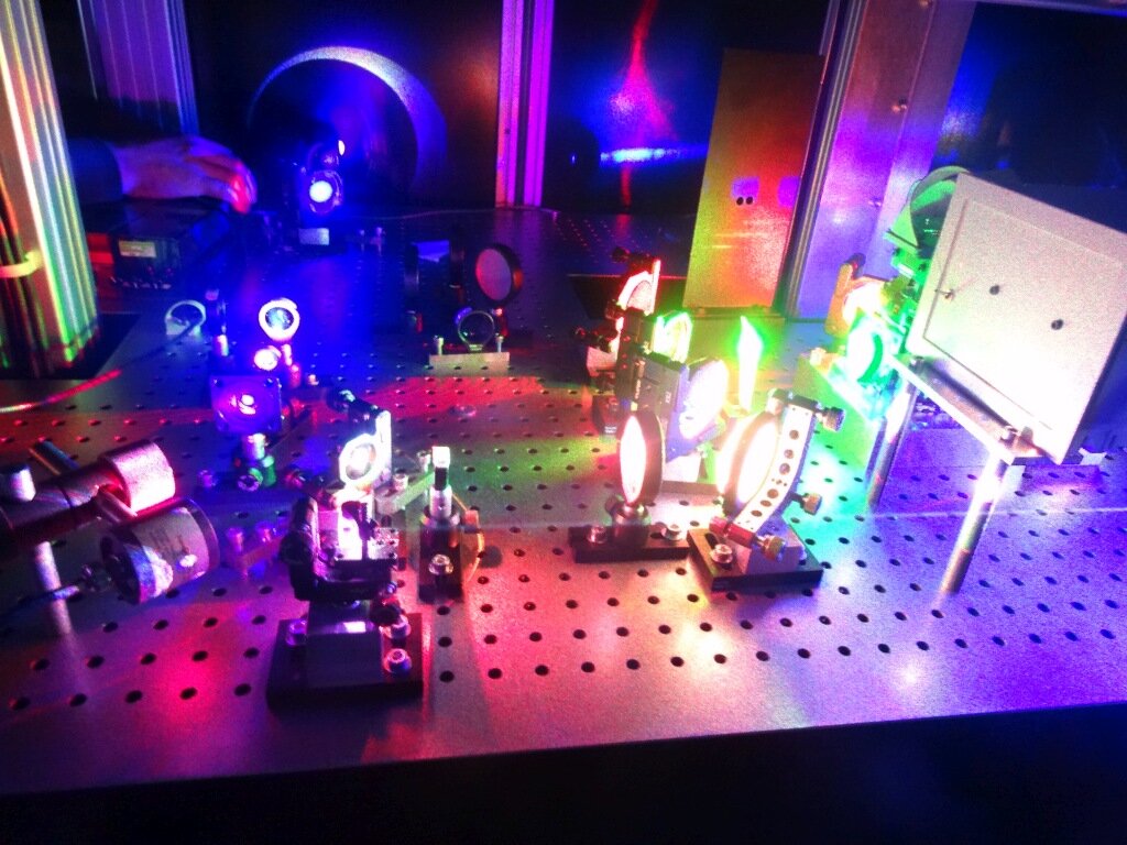
Credit: Johannes Zirkelbach/Max Planck Institute for the Science of Light


Topics: Applied Physics, Nanotechnology, Optics


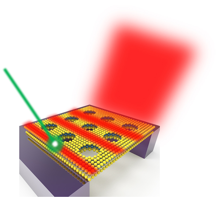
At the focus of a laser, a 100-nm-wide gold nanoparticle can block more than half the light. If additional particles are added, the amount of blocked light increases exponentially, as modeled by the Beer-Lambert law. But theorists predict that in the right set of circumstances, the addition of a molecule would, counterintuitively, decrease the light blocked—that is, make the nanoparticle partially transparent.


Vahid Sandoghdar of the Max Planck Institute for the Science of Light and his colleagues have now shown that predicted partial transparency for a near-field coupled dye molecule (red in image) and a plasmonic nanoparticle (gold). The phenomenon is a result of the interference between the light scattered from the two.


To achieve the required coupling, the dye molecule must be in a particular orientation and less than a wavelength away from the gold nanoparticle. Controlling those parameters is tricky, so Sandoghdar and his colleagues left them to chance. The researchers started with an array of nanoparticles and then coated it with a molten crystal doped with dibenzoterrylene (DBT) dye molecules. After the colorless crystal solidified, the result was a stochastic distribution of DBT molecules.


Their strong, distinctive fluorescence made the dye molecules easy to find optically. But the team members needed to verify that the molecule was near-field coupled to a nanoparticle. They identified a particle with two nearby DBT molecules and shined [a] tunable titanium: sapphire laser on it. The nanoparticle acts as an antenna, which enhances the molecules’ fluorescence. Relative to the other, one DBT molecule had telltale signatures of near-field interactions: enhanced and spectrally broadened fluorescence and a shorter excited-state lifetime—1.4 ns compared with the usual 8.1 ns.


Nanoparticle turns partially transparent, Heather Hill, Physics Today


Read more…

Fit...

20EL001_Exoskeleton-edit.jpg?profile=RESIZE_584x

Reflective markers are attached to blue 3D-printed apparatus above and below the user’s knee as well as two metal plates on the exoskeleton leg. Researchers track and compare the movement of the markers to gain insight into how well the exoskeletons fit. In this composite photo, the bottom plate has been added after the original image was taken to show the entire configuration.
Credit: N. Hanacek/NIST

Topics: Applied Physics, NIST, Research, Robotics

A shoddily tailored suit or a shrunken T-shirt may not be the most stylish, but wearing them is unlikely to hurt more than your reputation. An ill-fitting robotic exoskeleton on the battlefield or factory floor, however, could be a much bigger problem than a fashion faux pas. 

Exoskeletons, many of which are powered by springs or motors, can cause pain or injury if their joints are not aligned with the user. To help manufacturers and consumers mitigate these risks, researchers at the National Institute of Standards and Technology (NIST) developed a new measurement method to test whether an exoskeleton and the person wearing it are moving smoothly and in harmony. 

In a new report, the researchers describe an optical tracking system (OTS) not unlike the motion capture techniques used by filmmakers to bring computer-generated characters to life. 

The OTS uses special cameras that emit light and capture what is reflected back by spherical markers arranged on objects of interest. A computer calculates the position of the labeled objects in 3D space. Here, this approach was used to track the movement of an exoskeleton and test pieces, called “artifacts,” fastened to its user.

Exoskeleton Research Marches Forward With NIST Study on Fit, NIST

Read more…

Photography of the Invisible...

Figure

Figure 1. Sarah Frances Whiting (1847–1927) using a fluoroscope to examine the bones in her hand in Wellesley College’s physics laboratory, circa 1896. On the table in front of her is a Crookes tube mounted on a stand and an induction coil to modulate the voltage. (Courtesy of Wellesley College.)

Topics: Applied Physics, Optics, Women in Science, X-rays

In February 1896 Sarah Frances Whiting, founder of the physics and astronomy departments at Wellesley College, conducted a series of x-ray experiments. She was working only a few weeks after the public announcement of Wilhelm Röntgen’s discovery of the rays, and she was not alone; amateur and professional scientists at colleges, universities, and medical centers across the US were attempting to replicate and extend Röntgen’s results. But Whiting (see figure 1), who enlisted the assistance of a Wellesley colleague and several students, was among the first to do so successfully. Even more importantly, Whiting was the first woman—and almost certainly the first person, male or female—to do so in an undergraduate laboratory. Her original glass plates from the experiments do not survive, but 15 photographs printed from them (see the opening image of one such photo above) were recently rediscovered in a campus building slated for demolition. They provide a vivid reminder of Whiting’s success.

The x-ray experiments were only one instance in which Whiting drew on her keen engagement with contemporary scientific advances to offer her students an experience available to few undergraduates at the time, and to almost no women. Throughout her long career, Whiting introduced thousands of women to physics and astronomy, both fields then associated almost entirely with men. Her pedagogical efforts led many of her female students to pursue their own careers in the sciences.

Sarah Frances Whiting and the “photography of the invisible”

John S. Cameron is an emeritus professor of biological sciences and Jacqueline Marie Musacchio is a professor of art history at Wellesley College in Massachusetts.

Read more…

Comb on a Chip...


MoilleCover_v2-1.jpg
Experimental setup to generate a set of stable frequencies in a cryogenically cooled laser microresonator frequency comb. The ring-shaped microresonator, small enough to fit on a microchip, operates at very low laser power and is made from the semiconductor aluminum gallium arsenide.


Topics: Applied Physics, Instrumentation, NIST, Nanotechnology, Semiconductor Technology


Just as a meter stick with hundreds of tick marks can be used to measure distances with great precision, a device known as a laser frequency comb, with its hundreds of evenly spaced, sharply defined frequencies, can be used to measure the colors of light waves with great precision.

Small enough to fit on a chip, miniature versions of these combs — so named because their set of uniformly spaced frequencies resembles the teeth of a comb — are making possible a new generation of atomic clocks, a great increase in the number of signals traveling through optical fibers, and the ability to discern tiny frequency shifts in starlight that hint at the presence of unseen planets. The newest version of these chip-based “microcombs,” created by researchers at the National Institute of Standards and Technology (NIST) and the University of California at Santa Barbara (UCSB), is poised to further advance time and frequency measurements by improving and extending the capabilities of these tiny devices.

Comb on a Chip: New Design for ‘Optical Ruler’ Could Revolutionize Clocks, Telescopes, Telecommunications, NIST

Paper: G. Moille, L. Chang, W. Xie, A. Rao, X. Lu, M. Davanco, J.E. Bowers and K. Srinivasan. Dissipative Kerr Solitons in a III-V Microresonator. Laser and Photonics Reviews. June 2020. DOI: 10.1002/lpor.202000022

Read more…
Anna-Demming-4-May-2020.jpg
Next big thing:
Haifei Zhan and colleagues reckon that carbon nanothreads have a future in energy storage.
(Courtesy: Queensland University of Technology)


Topics: Applied Physics, Battery, Materials Science, Nanotechnology

Computational and theoretical studies of diamond-like carbon nanothreads suggest that they could provide an alternative to batteries by storing energy in a strained mechanical system. The team behind the research says that nanothread devices could power electronics and help with the shift towards renewable sources of energy.

The traditional go-to device for energy storage is the electrochemical battery, which predates even the widespread use of electricity. Despite centuries of technological progress and near ubiquitous use, batteries remain prone to the same inefficiencies and hazards as any device based on chemical reactions – sluggish reactions in the cold, the danger of explosion in the heat and the risk of toxic chemical leakages.

Another way of storing energy is to strain a material that then releases energy as it returns to its unstrained state. The strain could be linear like stretching and then launching a rubber band from your finger; or twisted, like a wind-up clock or toy. Over a decade ago, theoretical work done by researchers at the Massachusetts Institute of Technology suggested that strained chords made from carbon nanotubes could achieve impressive energy-storage densities, on account of the material’s unique  mechanical properties.

Diamond nanothreads could beat batteries for energy storage, theoretical study suggests

Anna Demmings, Physics World
Read more…

Open University...


gradient_img.png


Topics: Applied Physics, Education, Internet, Nanotechnology, STEM


Today poignantly, is the 50th anniversary of Earth Day. Some of us celebrate in willing self-isolation; others wish a repeat of the 1918 Influenza Pandemic by callously campaigning for others to die for an economy so wrought with inequality it cannot handle it's centennial equivalent.

A disclaimer note: Though these are unique times to say the least, this is not a support for fully online STEM education, though there can be some. Science for the most part is done in-person. I hope this is a bridge until we get to that again. It's hard to Zoom a breadboard circuit design or a laboratory set up.

Worldwide demand is growing for effective STEM (science, technology, engineering, and mathematics) education that can produce workers with technical skills. Online classes—affordable, flexible, and accessible—can help meet that demand. Toward that goal, some countries have developed national online higher-education platforms, such as XuetangX in China and Swayam in India. In 2015 eight top Russian universities collaborated to create the National Platform of Open Education, or OpenEdu. Professors from highly ranked departments produced courses for the platform that could then be used, for a fee, by resource-constrained universities. The courses comply with national standards and enable universities to serve more students by reducing the cost per pupil.

A new study from Igor Chirikov at the University of California, Berkeley, and his collaborators at Stanford and Cornell Universities and the National Research University Higher School of Economics in Moscow investigates the effectiveness of the OpenEdu program. The researchers looked at two metrics—effectiveness of instruction and cost savings—and found that the platform was successful on both fronts.


Online STEM courses can rival their in-person analogues
Christine Middleton, Physics Today

Read more…

So Much for Moore...

3nmpic1.png
Figure 1: Planar transistors vs finFETs vs nanosheet FET. Source: Samsung


Topics: Applied Physics, Electrical Engineering, Moore's Law, Nanotechnology, Semiconductor Technology


So much for the Moore's law limit. Although under current circumstances, the progression might be stalled by our current viral situation: the cost of chips will go higher, and consumers are currently making choices on food, jobs and toilet paper, not gadgets.

Select foundries are beginning to ramp up their new 5nm processes with 3nm in R&D. The big question is what comes after that.

Work is well underway for the 2nm node and beyond, but there are numerous challenges as well as some uncertainty on the horizon. There already are signs that the foundries have pushed out their 3nm production schedules by a few months due to various technical issues and the unforeseen pandemic outbreak, according to analysts. COVID-19 has slowed the momentum and impacted the sales in the IC industry.

This, in turn, is likely to push back the roadmaps beyond 3nm. Nevertheless, the current climate hasn’t stopped the semiconductor industry. Today, foundries and memory makers are running at relatively high fab utilization rates.

Behind the scenes, meanwhile, foundries and their customers continue to develop their 3nm and 2nm technologies, which are now slated for roughly 2022 and 2024, respectively. Work is also underway for 1nm and beyond, but that’s still far away.

Starting at 3nm, the industry hopes to make the transition from today’s finFET transistors to gate-all-around FETs. At 2nm and perhaps beyond, the industry is looking at current and new versions of gate-all-around transistors.

At these nodes, chipmakers will likely require new equipment, such as the next version of extreme ultraviolet (EUV) lithography. New deposition, etch and inspection/metrology technologies are also in the works.

Needless to say, the design and manufacturing costs are astronomical here. The design cost for a 3nm chip is $650 million, compared to $436.3 million for a 5nm device, and $222.3 million for 7nm, according to IBS. Beyond those nodes, it’s too early to say how much a chip will cost.


Making Chips At 3nm And Beyond
Mark Lapedus and Ed Sperling, Semiconductor Engineering

Read more…

Xenobots...


Topics: Applied Physics, Biology, Nanotechnology, Robotics


A team of researchers have built what they claim to be the first living robots. The “xenobots,” they say, can move, pick up objects, and even heal themselves after being cut.

The team is hoping the biological machines could one day be used to clean up microplastics in the ocean or even deliver drugs inside the human body, The Guardian reports.

To build the robots, the team used living cells from frog embryos and assembled them into primitive beings.

“These are novel living machines,” research co-lead Joshua Bongard, robotics expert at the University of Vermont, said in a statement. “They’re neither a traditional robot nor a known species of animal. It’s a new class of artifact: a living, programmable organism.”

The millimeter-length robots were designed by a supercomputer running an “evolutionary algorithm” that tested thousands of 3D designs for rudimentary life forms inside a simulation. The scientists then built a handful of the designs, which were able to propel themselves forward or fulfill a basic task inside the simulation using tweezers and cauterizing tools.

The tiny robots had about a week to ten days of “power” courtesy of living heart muscle cells that were able to expand and contract on their own.


Scientists Build “First Living Robots” From Frog Stem Cells
Victor Tangermann, Futurism

Read more…

Nonvolatile Charge Memory...

nonvolatile-charge-memory-device.jpg
Light irradiation-controlled nonvolatile charge memory. Left: schematic of the memory device. Right: the optical-controlled writing and erasing process of source-drain current. (Courtesy: Q Li et al J. Phys. D: Appl. Phys. 10.1088/1361-6463/ab5737)


Topics: Applied Physics, Device Physics, Electrical Engineering, Materials Science, Nanotechnology


Qinliang Li, Cailei Yuan and Ting Yu from Jiangxi Normal University, along with Qisheng Wang and Jingbo Li from South China Normal University, are developing nonvolatile charge memory devices with simple structures. Wang explains how the optically controllable devices combine the functions of light sensing and electrical storage.

The research is reported in full in Journal of Physics D: Applied Physics, published by IOP Publishing – which also publishes Physics World.

What was the motivation for the research and what problem were you trying to solve?


Nonvolatile memory devices are central to modern communication and information technology. Among various material systems, emerging two dimensional (2D) materials offer a promising platform for next-generation data-storage devices due to their unique planar structure and brilliant electronic properties. However, 2D materials-based nonvolatile memory devices have complicated architectures with multilayer stacking of 2D materials, metals, organics or oxides. This limits the capacity for device miniaturization, scalability and integration functionality.


In this work, we are trying to design a nonvolatile charge memory with simple device architecture. We also expect to explore a new type of optical control on the charge storage devices, which may bring us smart operation on data deposition and communication.


Nonvolatile charge memory device shows excellent room-temperature performance, Physics World
Qisheng Wang is professor at the Institute of Semiconductor Science and Technology, South China Normal University

Read more…

Transformers...


Topics: 3D Printing, Applied Physics, Research, Robotics, Soft Matter Physics


The researchers likely watched a lot of Saturday morning cartoons in the 1980s: original intro.

(CAMBRIDGE, Mass.) — The majority of soft robots today rely on external power and control, keeping them tethered to off-board systems or rigged with hard components. Now, researchers from the Harvard John A. Paulson School of Engineering and Applied Sciences (SEAS) and Caltech have developed soft robotic systems, inspired by origami, that can move and change shape in response to external stimuli, paving the way for fully untethered soft robots.

The research is published in Science Robotics.
 

3D-printed active hinges change shape in response to heat
Leah Burrows, SEAS Communications, Wyss Institute, Harvard

Read more…

Hologram Printer...

newprintercr.jpg
The new printer uses low-power continuous wave lasers to create holograms on a highly sensitive photomaterial developed by the researchers. Credit: C Yves GENTET


Topics: 3D Objects, 3D Printing, Applied Physics, Holograms, Optics, Research


Researchers have developed a new printer that produces digital 3-D holograms with an unprecedented level of detail and realistic color. The new printer could be used to make high-resolution color recreations of objects or scenes for museum displays, architectural models, fine art or advertisements that do not require glasses or special viewing aids.

"Our 15-year research project aimed to build a hologram printer with all the advantages of previous technologies while eliminating known drawbacks such as expensive lasers, slow printing speed, limited field of view and unsaturated colors," said research team leader Yves Gentet from Ultimate Holography in France. "We accomplished this by creating the CHIMERA printer, which uses low-cost commercial lasers and high-speed printing to produce holograms with high-quality color that spans a large dynamic range."


New printer creates extremely realistic colorful holograms, The Optical Society, Phys.org

Read more…

Twisted Fridge...

Twisted-fridge.jpg
Fridge-freezer: twistocaloric cooling could be coming to a kitchen near you. (Courtesy: iStock/Allevinatis)


Topics: Applied Physics, Green Tech, Research, Thermodynamics


A new refrigeration technology based on the twisting and untwisting of fibers has been demonstrated by a team led by Zunfeng Liu at Nankai University in China and Ray Baughman at the University of Texas at Dallas in the US. As the demand for refrigeration expands worldwide, their work could lead to the development of new cooling systems that do not employ gases that are harmful to the environment.

The cooling system relies on the fact that some materials undergo significant changes in entropy when deformed. As far back as 1805 – when the concepts of thermodynamics were first being developed – it was known that ordinary rubber heats up when stretched and cools down when relaxed. In principle, such mechanocaloric materials could be used in place of the gases that change entropy when compressed and expanded in commercial refrigeration systems. Replacing gas-based systems is an important environmental goal because gaseous refrigerants tend to degrade the ozone layer and are powerful greenhouse gases.

In their experiments, Liu and Baughman’s team studied the cooling effects of twist and stretch changes in twisted, coiled and supercoiled fibers of natural rubber, nickel-titanium and polyethylene fishing line. In each material, they observed a surface cooling as high as 16.4 °C, 20.8 °C, and 5.1 °C respectively, which they achieved through techniques including simultaneous releases of twisting and stretching, and unraveling bundles of multiple wires.


Refrigerator works by twisting and untwisting fibers, Materials, Physics World

Read more…

The Next FET...

CNTFET.png
Source: Modeling Carbon Nanotube FET Physics in COMSOL Multiphysics®
 

Topics: Applied Physics, Carbon Nanotubes, Field Effect Transistors, Nanotechnology


Silicon field-effect transistors (FETs) were developed in the late 1950s as a scaled-down, energy-efficient substitute for bipolar junction transistors. They paved the way for the high-density integrated circuits that today underlie most electronics (see the article by Alan Fowler, Physics Today, October 1993, page 59). With their lower gate voltages, carbon nanotube FETs could surpass silicon FET energy efficiency by nearly a factor of 10. In 2013 Subhasish Mitra, Max Shulaker (then at Stanford University), and coworkers made the first CNFET microprocessor; it comprised 178 transistors and could run a single operation.

Variability caused by the production process has made moving beyond that proof-of-concept computer challenging. Gage Hills, Christian Lau, and coworkers in Shulaker’s group at MIT have now overcome that hurdle with a protocol for wafer-scale CNFET microprocessor production. Their technique is also compatible with existing CMOS infrastructure, which lowers the bar for future commercial implementation.

To remove carbon nanotube aggregates—a common contaminant from CNT deposition on silicon wafers—the researchers spin-coated a layer of adhesive polymer over the device and then removed the aggregates using ultrasonic vibrations. In previous attempts, sonication damaged the nonaggregated CNTs. Using the photoresist binds them to the wafer, which preserves their function while removing more than 99% of the aggregates.


Production of carbon nanotube microprocessors gets scaled up
Christine Middleton, Physics Today

Read more…

Second Harmonic Microscopy...

1.5113727.figures.online.f1.jpg
Fig. 1 Typical geometry for the SH microscopy investigation of poled x-cut LNOI.


Topics: Applied Physics, Optical Physics, Thin Films


Abstract

Thin film lithium niobate has been of great interest recently, and an understanding of periodically poled thin films is crucial for both fundamental physics and device developments. Second-harmonic (SH) microscopy allows for the noninvasive visualization and analysis of ferroelectric domain structures and walls. While the technique is well understood in bulk lithium niobate, SH microscopy in thin films is largely influenced by interfacial reflections and resonant enhancements, which depend on film thicknesses and substrate materials. We present a comprehensive analysis of SH microscopy in x-cut lithium niobate thin films, based on a full three-dimensional focus calculation and accounting for interface reflections. We show that the dominant signal in backreflection originates from a copropagating phase-matched process observed through reflections, rather than direct detection of the counterpropagating signal as in bulk samples. We simulate the SH signatures of domain structures by a simple model of the domain wall as an extensionless transition from a −χ(2) to a +χ(2) region. This allows us to explain the main observation of domain structures in the thin-film geometry, and, in particular, we show that the SH signal from thin poled films allows to unambiguously distinguish areas, which are completely or only partly inverted in depth.


Second harmonic microscopy of poled x-cut thin film lithium niobate: Understanding the contrast mechanism
Journal of Applied Physics 126, 114105 (2019); https://doi.org/10.1063/1.5113727

Read more…

Nanocones...

Nanocones.jpg
A carbon nanocone includes nitrogen atoms around the periphery to improve the material’s solubility. Carbon atoms are shown in gray; hydrogen in white; nitrogen in blue; and oxygen in red.


Topics: Applied Physics, Chemistry, Graphene, Nanotechnology


Graphene, buckyballs, and carbon nanotubes now have a new family member, the nanocone, adding to the types of all-carbon nanostructures with remarkable electronic and optical characteristics and bringing its own promising properties. (J. Am. Chem. Soc., 2019, DOI: 10.1021/jacs.9b06617) Such molecules could be useful for developing efficient organic solar cells or as sensor molecules.

Organic chemist Frank Würthner and postdoctoral researcher Kazutaka Shoyama of the University of Würzburg came up with the method for synthesizing the nanocones, which are 1.68 nm in diameter and 0.432 nm tall. A five-atom ring of carbons forms the cone’s tip. The team used a cross-coupling annulation cascade to add hexagons around the edges of the ring until the molecule grew to 80 carbons. The team added five nitrogen atoms around the periphery of the cone, increasing the crystal’s solubility.


Nanocones extend the graphene toolbox, Neil Savage, Chemical & Engineering News

Read more…

Lamina Tenuissima...

thinnest-optical-device-2.jpg
Illustration of a tungsten disulfide monolayer suspended in air and patterned with a square array of nanoholes. Upon laser excitation, the monolayer emits photoluminescence. A portion of this light couples into the monolayer and is guided along the material. At the nanohole array, periodic modulation in the refractive index causes a small portion of the light to decay out of the plane of the material, allowing the light to be observed as guided mode resonance. Courtesy: E Cubukcu, UCSD


Note: lamina tenuissima = thinnest (Latin)

Topics: Applied Physics, Nanotechnology, Optical Physics, Photonics


Researchers have succeeded in making the thinnest ever optical device in the form of a waveguide just three atomic layers thick. The device could lead to the development of higher density optoelectronic chips.

Optical waveguides are crucial components in data communication technologies but scaling them down to the nanoscale has proved to be no easy task, despite important advances in nano-optics and nanomaterials. Indeed, the thinnest waveguide used in commercial applications today is hundreds of nanometres thick and researchers are studying nanowire waveguides down to 50 nm in the laboratory.

“We have now pushed this limit down to just three atoms thick,” says Ertugrul Cubukcu of the University of California at San Diego, who led this new research effort. “Such a thin waveguide, which is at the ultimate limit for how thin an optical waveguide can be built, might potentially lead to a higher density of waveguides or optical elements on an optoelectronic chip – in the same way that ever smaller transistors have led to a higher density of these devices on an electronic chip.”

Cubukcu and colleagues’ waveguide is just six angstroms thick. This makes it 104 times thinner than a typical optical fiber and about 500 times thinner than on-chip optical waveguides in integrated photonic circuits.


Three-atom-thick optical waveguide is the thinnest ever, Belle Dumé, Physics World

Read more…

Cyclocarbon...

5d568358294db.jpg
From left to right, precursor molecule C24O6, intermediates C22O4 and C20O2 and the final product cyclo [18]carbon C18 created on surface by dissociating CO masking groups using atom manipulation. The bottom row shows atomic force microscopy (AFM) data using a CO functionalized tip. Credit: IBM Research


Topics: Applied Physics, Atomic Force Microscopy, Chemistry, Nanotechnology, Research


A team of researchers from Oxford University and IBM Research has for the first time successfully synthesized the ring-shaped multi-carbon compound cyclocarbon. In their paper published in the journal Science, the group describes the process they used and what they learned about the bonds that hold a cyclocarbon together.

Carbon is one of the most abundant elements, and has been found to exist in many forms, including diamonds and graphene. The researchers with this new effort note that much research has been conducted into the more familiar forms (allotropes) how they are bonded. They further note that less well-known types of carbon have not received nearly as much attention. One of these, called cyclocarbon, has even been the topic of debate. Are the two-neighbor forms bonded by the same length bonds, or are there alternating bonds of shorter and longer lengths? The answer to this question has been difficult to find due to the high reactivity of such forms. The researchers with this new effort set themselves the task of finding the answer once and for all.

The team's approach involved creating a precursor molecule and then whittling it down to the desired form. To that end, they used atomic force microscopy to create linear lines of carbon atoms atop a copper substrate that was covered with salt to prevent the carbon atoms from bonding with the subsurface. They then joined the lines of atoms to form the carbon oxide precursor C24O6, a triangle-shaped form. Next, the team applied high voltage through the AFM to shear off one of the corners of the triangle, resulting in a C22O4 form. They then did the same with the other two corners. The result was a C18 ring—an 18-atom cyclocarbon. After creating the ring, the researchers found that the bonds holding it together were the alternating long- and short-type bonds that had been previously suggested.


Ring-shaped multi-carbon compound cyclocarbon synthesized, Bob Yirka , Phys.org

Read more…

Smart Packaging...

PWNANOApr18-pragmatIC-wafer-image.jpg
Cheaper flexible integrated circuits open up new markets. (Courtesy: PragmatIC)


Topics: Applied Physics, Moore's Law, Semiconductor Technology, Nanotechnology


For more than 50 years, progress in the electronics industry has been guided by Moore’s law: the idea that the number of transistors in a silicon-based integrated circuit (IC) will double approximately every 18 months. The consequences of this doubling include a continual reduction in the size of silicon ICs, as it becomes possible to provide increasingly complex and high-performance functionality in smaller and smaller areas of silicon, and at progressively lower cost relative to the circuits’ processing power.

Moore’s law is an empirical rule of thumb rather than a robust physical principle, and much has been written about how, why and when it will eventually fail. But even before we reach that point, manufacturers are already finding that, in practice, the cost savings associated with reducing the size, or “footprint”, of ICs will only carry them so far. The reason is that below a certain minimum size, ICs become difficult to handle easily or effectively. For highly complex circuitry, such as that found in computers with many millions of transistors in a single IC, this limit on handling size may not be a consideration. However, for applications that require less complex circuits, the size constraint imposed by the physical aspect of handling ICs becomes a limiting factor in their cost.

The approach we have taken at PragmatIC is to use thin, flexible substrates, rather than rigid silicon, as the base for building our circuits. The low cost of the materials involved and the relatively low complexity of our target applications alters the economics around circuit footprint and overall IC cost. Accepting a larger footprint can lower capital expenditure because it means that ultrahigh-end precision tooling is not required to fabricate our circuits during the manufacturing process. In turn, for low-complexity applications, this can lead to a lower final IC cost.

The resulting flexible integrated circuits, or FlexICs, are thinner than a human hair, so they can easily be embedded in everyday objects. They also cost around 10 times less than silicon ICs, making it economically viable for them to appear in trillions of smart objects that engage with consumers and their environments. Since the technology was developed, PragmatIC FlexICs have been trialed in a wide variety of markets, including consumer goods, games, retail, and the pharmaceutical and security sectors.


A smart approach to smart packaging
Catherine Ramsdale is vice-president of device development at PragmatIC

Read more…

LMADIS...

Topics: Applied Physics, Electromagnetic Radiation, Politics, Robotics


I normally cheer the usage and applications of recent technology. In light of recent events, this may not be a swift idea. The second through fourth letters of the acronym are quite (and maybe intentionally) ominous.

"War is the continuation of politics by other means." Carl von Clausewitz


*****


In June, Iran’s military shot down one of the U.S. Navy’s $130 million Global Hawk drones, claiming it had veered out of international airspace and into the nation’s territory.

Now, the U.S. Navy has returned the favor, using a new directed-energy weapon to disable an Iranian drone in the same region — marking the next-generation device’s first known “kill.”

According to a Department of Defense statement, a fixed wing drone approached the USS Boxer while the ship traveled through the Strait of Hormuz on July 18. The drone then came within a threatening range, prompting the crew to take “defensive action.”

A defense official later told Military.com on the condition of anonymity that the Navy took out the drone using its Light Marine Air Defense Integrated System (LMADIS), a new device that uses radio frequencies to jam drones.

Iran’s Minister of Foreign Affairs Mohammad Javad Zarif, meanwhile, has denied the incident altogether, telling reporters the nation has “no information about losing a drone.”


US Navy's Weapon Gets First "Kill," Shoots Down Iranian Drone
Kristin Houser, Futurism

Read more…

Your iPhone as Tricorder...

Silicon chips similar to those that would be used in the detection process. Credit: Vanderbilt University/Heidi Hall


Topics: Applied Physics, Medical Physics, Nanotechnology, Star Trek


The simplest home medical tests might look like a deck of various silicon chips coated in special film, one that could detect drugs in the blood, another for proteins in the urine indicating infection, another for bacteria in water and the like. Add the bodily fluid you want to test, take a picture with your smart phone, and a special app lets you know if there's a problem or not.

That's what electrical engineer Sharon Weiss, Cornelius Vanderbilt Professor of Engineering at Vanderbilt University, and her students developed in her lab, combining their research on low-cost, nanostructured thin films with a device most American adults already own. "The novelty lies in the simplicity of the basic idea, and the only costly component is the smart phone," Weiss said.

"Most people are familiar with silicon as being the material inside your computer, but it has endless uses," she said. "With our nanoscale porous silicon, we've created these nanoscale holes that are a thousand times smaller than your hair. Those selectively capture molecules when pre-treated with the appropriate surface coating, darkening the silicon, which the app detects."


iPhone plus nanoscale porous silicon equals cheap, simple home diagnostics
Heidi Hall, Vanderbilt University, Phys.org

Read more…