 |
| Source: Modeling Carbon Nanotube FET Physics in COMSOL Multiphysics® |
Topics: Applied Physics, Carbon Nanotubes, Field Effect Transistors, Nanotechnology
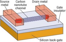
Silicon field-effect transistors (FETs) were developed in the late 1950s as a scaled-down, energy-efficient substitute for bipolar junction transistors. They paved the way for the high-density integrated circuits that today underlie most electronics (see the article by Alan Fowler, Physics Today, October 1993, page 59). With their lower gate voltages, carbon nanotube FETs could surpass silicon FET energy efficiency by nearly a factor of 10. In 2013 Subhasish Mitra, Max Shulaker (then at Stanford University), and coworkers made the first CNFET microprocessor; it comprised 178 transistors and could run a single operation.
Variability caused by the production process has made moving beyond that proof-of-concept computer challenging. Gage Hills, Christian Lau, and coworkers in Shulaker’s group at MIT have now overcome that hurdle with a protocol for wafer-scale CNFET microprocessor production. Their technique is also compatible with existing CMOS infrastructure, which lowers the bar for future commercial implementation.
To remove carbon nanotube aggregates—a common contaminant from CNT deposition on silicon wafers—the researchers spin-coated a layer of adhesive polymer over the device and then removed the aggregates using ultrasonic vibrations. In previous attempts, sonication damaged the nonaggregated CNTs. Using the photoresist binds them to the wafer, which preserves their function while removing more than 99% of the aggregates.
Production of carbon nanotube microprocessors gets scaled up
Christine Middleton, Physics Today