materials_science (14)

Graphene Currents...

237921_web.jpg

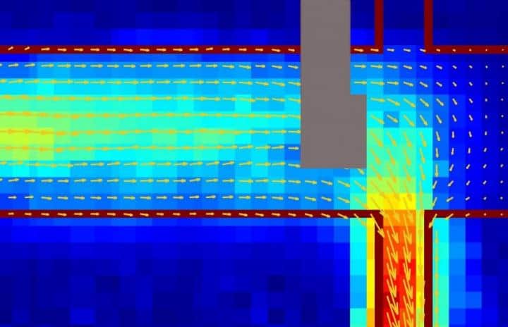
A picture of an electrical current in graphene (marked by the red outline) showing a fluid-like flow imaged using a diamond-based quantum sensor. The grey portion is where the metal electrical contacts prevented collection of data. Courtesy: Walsworth and Yacoby research groups, Harvard and University of Maryland

Topics: Materials Science, Nanotechnology, Quantum Mechanics, Semiconductor Technology

A team led by researchers from Harvard University and the University of Maryland in the US has used defects in diamond to map the magnetic field generated by electrical currents in graphene. Their experiments reveal that currents in this atomically-thin form of carbon flow like a viscous fluid – a result that could provide fresh insights into the collective behavior of electrons in strongly-interacting quantum systems.</em>

Graphene has many exceptional electrical properties. Among them is the fact that, at the point where its conduction and valence bands just touch each other (the Dirac point), it can support currents composed of electrons and an equal number of positively-charged holes, rather than electrons alone. In the present work, Ronald WalsworthAmir Yacoby and colleagues set out to establish whether these electron-hole plasmas (or Dirac fluids, as they are also known) flow smoothly, like electrons traveling through a metallic wire, or unevenly like water running through a pipe.

Diamond defects reveal viscous currents in graphene, Isabelle Dumé, Physics World

Read more…

APS...

Topics: COVID-19, Materials Science, Optics, Photonics, Research

From chemistry to materials science to COVID-19 research, the APS is one of the most productive X-ray light sources in the world. An upgrade will make it a global leader among the next generation of light sources, opening new frontiers in science.

In the almost 25 years since the Advanced Photon Source (APS), a U.S. Department of Energy (DOE) Office of Science User Facility, first opened at DOE’s Argonne National Laboratory, it has played an essential role in some of the most pivotal discoveries and advancements in science.

More than 5,000 researchers from around the world conduct experiments at the APS every year, and their work has, among many other notable successes, paved the way for better renewable batteries; resulted in the development of numerous new drugs; and helped to make vehicles more efficient, infrastructure materials stronger and electronics more powerful.

Advanced Photon Source Upgrade will transform the world of scientific research, Brett Hansard, Argonne National Laboratory

Read more…

CdTe and IoT...

Cell_testing_1.jpg

The thin-film materials being tested during development. Courtesy: I Mathews

Topics: Alternate Energy, Internet of Things, Materials Science, Solar Power

Photovoltaic cells made from cadmium telluride (CdTe) – already widely used in solar energy generation – also excel at harvesting ambient light indoors, making them an excellent energy source for the fast-growing Internet of Things (IoT). This is the finding of researchers at the Massachusetts Institute of Technology (MIT) in the US and the Tyndall National Institute at the University of Cork, Ireland, who fabricated low-cost CdTe cells and measured their photovoltaic response when exposed to light from various sources, including LED bulbs.

At present, indoor IoT devices such as wireless sensors are typically powered by batteries.  However, study lead author Ian Mathews says that photovoltaic cells would be better because of they require less maintenance and are cheaper and easier to make. In his view, these characteristics present a “significant market opportunity” for CdTe cells in particular, yet researchers have rarely tested their effectiveness at converting ambient light (from incandescent, compact fluorescence, or LED bulbs, for example) into electrical energy. Instead, previous studies of indoor-light energy generation have mainly focused on rival photovoltaic technologies, such as silicon, III-V semiconductors, organic PV devices, and perovskite materials.

Thin-film solar cells make champion harvesters of ambient lightIsabelle Dumé, Physics World

Read more…

Quantum Phase Battery...

zoom-1-light.jpg
The first quantum phase battery, consisting of an indium arsenide (InAs) nanowire in contact with aluminium superconducting leads. (Courtesy: Andrea Iorio)


Topics: Battery, Cooper Pairs, Materials Science, Quantum Mechanics, Superconductivity

Researchers in Spain and Italy have constructed the first-ever quantum phase battery – a device that maintains a phase difference between two points in a superconducting circuit. The battery, which consists of an indium arsenide (InAs) nanowire in contact with aluminium (Al) superconducting leads, could be used in quantum computing circuits. It might also find applications in magnetometry and highly sensitive detectors based on superconductors.

In a classical battery (also known as the Volta pile), chemical energy is converted into a voltage difference. The resulting current flow can then be used to power electronic circuits. In quantum circuits and devices based on superconducting materials, however, current may flow without an applied external voltage, thus dispensing with the need for a classical battery.

The concept of a quantum phase battery was studied theoretically in 2015 by Sebastián Bergeret of the Material Physics Center (CFM-CSIC) and Ilya Tokatly at the University of the Basque Country in Donostia-San Sebastián, Spain. Their battery design comprised a combination of superconducting and magnetic materials and was based on a Josephson junction – a non-superconducting region through which the Cooper pairs responsible for superconductivity can tunnel. This semiconducting “weak link” provides a persistent phase difference between the superconductors in the circuit, similar to the way that a classical battery provides a persistent voltage drop in an electronic circuit. Thanks to this phase difference, a superconducting current (that is, a current with zero dissipation) flows when the junction is embedded in the superconducting circuit.

Physicists create quantum phase battery, Isabelle Dumé, Physics World

Read more…

Armored Surfaces...

233357_web.jpg
A schematic representation of how the surface looks, and how the structure repels water. Courtesy: Aalto University


Topics: Materials Science, Nanotechnology, Surface Engineering

A micron-scale “armor” that protects highly water-repellent nanostructures from damage has been developed by researchers in China and Finland. The new extra-durable coating could make it possible to employ these “superhydrophobic” surfaces on devices such as solar panels and vehicle windscreens that experience tough environmental conditions.

As their name suggests, superhydrophobic materials repel water extremely well. They owe this impressive ability to a thin layer of air that develops around nanometre-scale structures on their surface. By ensuring that droplets barely touch the solid part of the surface at all, the air layer effectively acts as a lubricant, allowing water droplets to roll off with near-zero friction.

These nanostructured surfaces are, however, mechanically fragile and can easily be wiped away. To address this drawback, a research team led by Xu Deng of the University of Electronic Science and Technology of China in Chengdu and Robin Ras of Finland’s Aalto University created a superhydrophobic surface containing structures at two different length scales: a nanoscale structure that is water repellent and a microscale one that provides durability.

The microstructure consists of an interconnected frame containing “pockets” of tiny inverted pyramids. Within these pyramids are the highly water-repellent and mechanically fragile nanostructures. The frame thus acts as a shield, preventing the nanostructure coating from being removed by abradants larger than the frame. “A finger, screwdriver or even sandpaper glides over these microstructures, leaving the nanostructures untouched, thereby preserving the surface’s attractive water-repellent feature,” Ras says.

Superhydrophobic surfaces toughen up, Isabelle Dumé, Physics World

Read more…

2D Boost for 5G...

v5_Kim1a_green-724x1024.jpg
A diagram of the UT Austin team's switch showing two gold electrodes with a layer of hBN in between. (Courtesy: UT Austin)


Topics:  Boron Nitride, Internet of Things, Materials Science, Nanotechnology

Two-dimensional sheets of boron nitride can be used to create an analogue switch that gives communication devices more efficient access to radio, 5G and terahertz frequencies while increasing their battery life. The switch, which was developed by a team of researchers at the University of Texas at Austin in the US and the University of Lille in France, could be employed in a host of different applications, including smartphones, mobile systems and the “Internet of things”.

Analogue switches are routinely employed in communication systems to switch from one frequency band to another, route signals between transmitting and receiving antennas, and reconfigure wireless networks. Traditionally, these switches are based on solid-state diodes or transistors, but components of this type consume energy even in standby mode, reducing the battery life of the device. With 5G networking set to drive a tenfold increase in data throughput – enabling advances in self-driving cars, delivery drones, remote surgery and fast downloads of high-definition media in the process – addressing this energy drain is more urgent than ever.

5G switching gets a 2D boost, Isabelle Dumé, Physics World

Read more…

Photonic Nanojets...

5.0007611.figures.online.f1.jpeg
FIG. 1. (a) Long-legs cellar spider. (b) Reeling mechanism. (c) Manufacturing process of decorating spider silk. (d) Spider silk with dome lens placed on a dedicated holder. (e) Microphotograph of dome lens. (f) Laser scanning digital microscope system for measuring dome lens. (g) Schematic diagram of the dome lens for generating PNJ.


Topics: Biology, Materials Science, Nanotechnology

ABSTRACT

In this work, we thoroughly investigate the shape, size, and location of the photonic nanojets (PNJs) generated from the illuminated dome lens. The silk fiber is directly extracted from the cellar spider and used to form the dome lens by its liquid-collecting ability. The solidified dielectric dome lenses with different dimensions are obtained by using ultraviolet curing. Numerical and experimental results show that the long PNJs are strongly modulated by the dimension of the dome lens. The optimal PNJ beam shaping is achieved by using a mesoscale dielectric dome lens. The PNJ with a long focal length and a narrow waist could be used to scan over a target for large-area imaging. The silk fiber with a dome lens is especially useful for bio-photonic applications by combining its biocompatibility and flexibility.

Optimal photonic nanojet beam shaping by mesoscale dielectric dome lens

Journal of Applied Physics 127, 243110 (2020); https://doi.org/10.1063/5.0007611

C.B. Lin, Yi-Ting Lee, and Cheng-Yang Liu

Read more…

"A Whole New Universe"...

d41586-020-01658-1_18045322.jpg
A Cryo-EM map of the protein apoferritin. Credit: Paul Emsley/MRC Laboratory of Molecular Biology


Topics: Biology, Cryogenic-Electron Microscopy, Materials Science, Nanotechnology

A game-changing technique for imaging molecules known as cryo-electron microscopy has produced its sharpest pictures yet — and, for the first time, discerned individual atoms in a protein.

By achieving atomic resolution using cryogenic-electron microscopy (cryo-EM), researchers will be able to understand, in unprecedented detail, the workings of proteins that cannot easily be examined by other imaging techniques, such as X-ray crystallography.

The breakthrough, reported by two laboratories late last month, cements cryo-EM’s position as the dominant tool for mapping the 3D shapes of proteins, say scientists. Ultimately, these structures will help researchers to understand how proteins work in health and disease, and lead to better drugs with fewer side effects.

“It’s really a milestone, that’s for sure. There’s really nothing to break anymore. This was the last resolution barrier,” says Holger Stark, a biochemist and electron microscopist at the Max Planck Institute for Biophysical Chemistry in Göttingen, Germany, who led one of the studies1. The other2 was led by Sjors Scheres and Radu Aricescu, structural biologists at the Medical Research Council Laboratory of Molecular Biology (MRC-LMB) in Cambridge, UK. Both were posted on the bioRxiv preprint server on 22 May.

“True ‘atomic resolution’ is a real milestone,” adds John Rubinstein, a structural biologist at the University of Toronto in Canada. Getting atomic-resolution structures of many proteins will still be a daunting task because of other challenges, such as a protein’s flexibility. "These preprints show where one can get to if those other limitations can be addressed,” he adds.

‘It opens up a whole new universe’: Revolutionary microscopy technique sees individual atoms for first time

Ewen Callaway, Nature

Read more…

Kondo Effect...

227888.jpg
Daniel Mazzone led the project to explore the mechanism that causes samarium sulphide to expand dramatically when cooled. Credit: Brookhaven National Laboratory


Topics: Materials Science, Quantum Mechanics, Research, Thermodynamics

Most metals expand when heated and contract when cooled. A few metals, however, do the opposite, exhibiting what’s known as negative thermal expansion (NTE). A team of researchers led by Ignace Jarrige and Daniel Mazzone of Brookhaven National Laboratory in the US has now found that in one such metal, yttrium-doped samarium sulphide (SmS), NTE is linked to a quantum many-body phenomenon called the Kondo effect. The work could make it possible to develop alloys in which positive and negative expansion cancel each other out, producing a composite material with a net-zero thermal expansion – a highly desirable trait for applications in aerospace and other areas of hi-tech manufacturing.

Even within the family of NTE materials, yttrium-doped SmS is an outlier, gradually expanding by up to 3% when cooled over a few hundred degrees. To better understand the mechanisms behind this “giant” NTE behavior, Mazzone and Jarrige employed X-ray diffraction and spectroscopy to investigate the material’s electronic properties.

The researchers carried out the first experiments at the Pair Distribution Function (PDF) beamline at Brookhaven’s National Synchrotron Light Source (II) (NSLS-II). They placed their SmS sample inside a liquid-helium cooled cryostat in the beam of the synchrotron X-rays and measured how the X-rays scattered off the electron clouds around the atomic ions. By tracking how these X-rays scatter, they identified the locations of the atoms in the crystal structure and the spacings between them.

“Our results show that, as the temperature drops, the atoms of this material move farther apart, causing the entire material to expand by up to 3% in volume,” says Milinda Abeykoon, the lead scientist on the PDF beamline.

Kondo effect induces giant negative thermal expansion, Belle Dumé, Physics World

Read more…
Anna-Demming-4-May-2020.jpg
Next big thing:
Haifei Zhan and colleagues reckon that carbon nanothreads have a future in energy storage.
(Courtesy: Queensland University of Technology)


Topics: Applied Physics, Battery, Materials Science, Nanotechnology

Computational and theoretical studies of diamond-like carbon nanothreads suggest that they could provide an alternative to batteries by storing energy in a strained mechanical system. The team behind the research says that nanothread devices could power electronics and help with the shift towards renewable sources of energy.

The traditional go-to device for energy storage is the electrochemical battery, which predates even the widespread use of electricity. Despite centuries of technological progress and near ubiquitous use, batteries remain prone to the same inefficiencies and hazards as any device based on chemical reactions – sluggish reactions in the cold, the danger of explosion in the heat and the risk of toxic chemical leakages.

Another way of storing energy is to strain a material that then releases energy as it returns to its unstrained state. The strain could be linear like stretching and then launching a rubber band from your finger; or twisted, like a wind-up clock or toy. Over a decade ago, theoretical work done by researchers at the Massachusetts Institute of Technology suggested that strained chords made from carbon nanotubes could achieve impressive energy-storage densities, on account of the material’s unique  mechanical properties.

Diamond nanothreads could beat batteries for energy storage, theoretical study suggests

Anna Demmings, Physics World
Read more…

Interphase...

Battery%2BSeparator%2Band%2BElectrolyte.JPG
Intro to Nano Energy: Lecture 5


Topics: Battery, Materials Science, Nanotechnology


What happens in a lithium-ion battery when it first starts running? A complex series of events, it turns out – from electrolytic ion reorganization to a riot of chemical reactions. To explore this early part of a battery’s life, researchers in the US have monitored a battery’s chemical evolution at the electrode surface. Their work could lead to improved battery design by targeting the early stages of device operation.

The solid-electrolyte interphase is the solid gunk that materializes around the anode. Borne from the decomposition of the electrolyte, it is crucial for preventing further electrolyte degradation by blocking electrons while allowing lithium ions to pass through to complete the electrical circuit.

The solid-electrolyte interphase does not appear immediately. When a lithium ion battery first charges up, the anode repels anions and attracts positive lithium ions, separating oppositely charged ions into two distinct layers. This electric double layer dictates the eventual composition and structure of the solid-electrolyte interphase.


Emergence of crucial interphase in lithium-ion batteries is observed by researchers
Shi En Kim, Physics World

Read more…

Nonvolatile Charge Memory...

nonvolatile-charge-memory-device.jpg
Light irradiation-controlled nonvolatile charge memory. Left: schematic of the memory device. Right: the optical-controlled writing and erasing process of source-drain current. (Courtesy: Q Li et al J. Phys. D: Appl. Phys. 10.1088/1361-6463/ab5737)


Topics: Applied Physics, Device Physics, Electrical Engineering, Materials Science, Nanotechnology


Qinliang Li, Cailei Yuan and Ting Yu from Jiangxi Normal University, along with Qisheng Wang and Jingbo Li from South China Normal University, are developing nonvolatile charge memory devices with simple structures. Wang explains how the optically controllable devices combine the functions of light sensing and electrical storage.

The research is reported in full in Journal of Physics D: Applied Physics, published by IOP Publishing – which also publishes Physics World.

What was the motivation for the research and what problem were you trying to solve?


Nonvolatile memory devices are central to modern communication and information technology. Among various material systems, emerging two dimensional (2D) materials offer a promising platform for next-generation data-storage devices due to their unique planar structure and brilliant electronic properties. However, 2D materials-based nonvolatile memory devices have complicated architectures with multilayer stacking of 2D materials, metals, organics or oxides. This limits the capacity for device miniaturization, scalability and integration functionality.


In this work, we are trying to design a nonvolatile charge memory with simple device architecture. We also expect to explore a new type of optical control on the charge storage devices, which may bring us smart operation on data deposition and communication.


Nonvolatile charge memory device shows excellent room-temperature performance, Physics World
Qisheng Wang is professor at the Institute of Semiconductor Science and Technology, South China Normal University

Read more…

2D MXenes...

solar-farm-662095604-iStock_Milos-Muller.jpg
Helper two-dimensional metal-carbide layers could improve perovskite solar cell stability and help make these complex solar cells a viable green energy option. Credit: iStock Milos-Muller


Topics: Condensed Matter Physics, Green Tech, Materials Science, Metamaterials, Nanotechnology, Solar Power


With the reality of climate change looming, the importance of realistic green energy sources is higher than ever. Solar cells are one promising avenue, as they can convert readily available visible and ultraviolet energy into usable electricity. In particular, perovskite materials sandwiched between other support layers have demonstrated impressive power conversion efficiencies. Current challenges reside in optimizing perovskite/support layer interfaces, which can directly impact power conversion and cell degradation. Researchers Antonio Agresti et al. under the direction of Aldo Di Carlo at the University of Rome Tor Vergata in Italy have investigated how cells containing two-dimensional titanium-carbide MXene support layers could improve perovskite solar cell performance.

To obtain good power conversion within a perovskite solar cell, all layers and layer interfaces within the cell must have good compatibility. Typical cells contain the active perovskite material sandwiched between two charge transport layers, which are then adjacent to their corresponding electrodes. Support layers may also be added. Charge mobility, energy barriers, interface energy alignment, and interfacial vacancies all impact compatibility and subsequent cell performance and stability. Thus, engineering well-suited interfaces with the cell is paramount to cell success and long-term stability, an important criterion for potential commercialization.

Two-dimensional buffer materials could help to modify and promote useful interface interactions. MXenes, a growing class of two-dimensional transitional metal carbides, nitrides, and carbonitrides, have shown impressive electronic properties that are easily tuned via surface modification. For example, the band gap of an MXene can be modified by changing the surface termination group from an oxygen atom to a hydroxide molecule. Additionally, MXene composition impacts the overall material performance. This type of fine-tuning allows impressive control over MXene properties and makes them ideal for interface adjustments.


Two-dimensional MXenes improve perovskite solar cell efficiency
Amanda Carr, Physics World

#P4TC: MXenes...August 24, 2015

Read more…

Boiling Superconductivity...

Hydride.png
Under pressure: calculated structure of lithium magnesium hydride. Lithium atoms appear in green, magnesium in blue and hydrogen in red. (Courtesy: Ying Sun et al/Phys. Rev. Lett.)


Topics: Chemistry, Materials Science, Nanotechnology, Superconductors


A material that remains a superconductor when heated to the boiling point of water has been predicted by physicists in China. Hanyu Liu, Yanming Ma and colleagues at Jilin University have calculated that lithium magnesium hydride will superconduct at temperatures as high as 473 K (200 °C).

The catch is that the hydrogen-rich material must be crushed at 250 GPa, which is on par with pressures at the center of the Earth. While such a pressure could be achieved in the lab, it would be very difficult to perform an experiment to verify the prediction. The team’s research could, however, lead to the discovery of more practical high-temperature superconductors.

Superconductors are materials that, when cooled below a critical temperature, will conduct electricity with zero resistance. Most superconductors need to be chilled to very low temperatures, so the holy grail of superconductivity research is to find a substance that will superconduct at room temperature. This would result in lossless electricity transmission and boost technologies that rely on the generation or detection of magnetic fields.


Superconductivity at the boiling temperature of water is possible, say physicists
Hamish Johnston, Physics World

Read more…