thin_films (2)

Second Harmonic Microscopy...

1.5113727.figures.online.f1.jpg
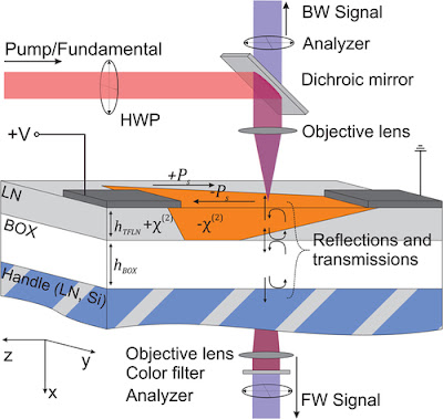
Fig. 1 Typical geometry for the SH microscopy investigation of poled x-cut LNOI.


Topics: Applied Physics, Optical Physics, Thin Films


Abstract

Thin film lithium niobate has been of great interest recently, and an understanding of periodically poled thin films is crucial for both fundamental physics and device developments. Second-harmonic (SH) microscopy allows for the noninvasive visualization and analysis of ferroelectric domain structures and walls. While the technique is well understood in bulk lithium niobate, SH microscopy in thin films is largely influenced by interfacial reflections and resonant enhancements, which depend on film thicknesses and substrate materials. We present a comprehensive analysis of SH microscopy in x-cut lithium niobate thin films, based on a full three-dimensional focus calculation and accounting for interface reflections. We show that the dominant signal in backreflection originates from a copropagating phase-matched process observed through reflections, rather than direct detection of the counterpropagating signal as in bulk samples. We simulate the SH signatures of domain structures by a simple model of the domain wall as an extensionless transition from a −χ(2) to a +χ(2) region. This allows us to explain the main observation of domain structures in the thin-film geometry, and, in particular, we show that the SH signal from thin poled films allows to unambiguously distinguish areas, which are completely or only partly inverted in depth.


Second harmonic microscopy of poled x-cut thin film lithium niobate: Understanding the contrast mechanism
Journal of Applied Physics 126, 114105 (2019); https://doi.org/10.1063/1.5113727

Read more…
Superconductors' never-ending flow of electrical current could provide new options for energy storage and superefficient electrical transmission and generation. But the signature zero electrical resistance of superconductors is reached only below a certain critical temperature and is very expensive to achieve. Physicists in Serbia believe they've found a way to manipulate superthin, waferlike monolayers of superconductors, thus changing the material's properties to create new artificial materials for future devices. This image shows a liquid phase graphene film deposited on PET substrate. Credit: Graphene Laboratory, University of Belgrade


Topics: Applied Physics, Superconductors, Thin Films


Superconductors' never-ending flow of electrical current could provide new options for energy storage and superefficient electrical transmission and generation, to name just a few benefits. But the signature zero electrical resistance of superconductors is reached only below a certain critical temperature, hundreds of degrees Celsius below freezing, and is very expensive to achieve.

Physicists from the University of Belgrade in Serbia believe they've found a way to manipulate superthin, waferlike monolayers of superconductors, such as graphene, a monolayer of carbon, thus changing the material's properties to create new artificial materials for future devices. The findings from the group's theoretical calculations and experimental approaches are published in the Journal of Applied Physics.

"The application of tensile biaxial strain leads to an increase of the critical temperature, implying that achieving high temperature superconductivity becomes easier under strain," said the study's first author from the University of Belgrade's LEX Laboratory, Vladan Celebonovic.


Strain enables new applications of 2-D materials, Phys.org

Read more…