 |
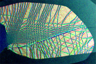
| Credit: Muller lab Three dark field-transmission electron microscopy images of bilayer graphene are overlaid with colors to show diffraction angles. The lines are soliton boundaries. |
By Anne Ju
Just an atom thick, 200 times stronger than steel and a near-perfect conductor, graphene’s future in electronics is all but certain. But to make this carbon supermaterial useful, it needs to be a semiconductor – a material that can switch between insulating and conducting states, which forms the basis for all electronics today.
Combining experiment and theory, Cornell researchers have moved a step closer to making graphene a useful, controllable material. They showed that when grown in stacked layers, graphene produces some specific defects that influence its conductivity.
On the experiment side, a research group has imaged and analyzed the structure and behavior of graphene sheets stacked one on top of the other, called bilayer graphene. The group, publishing online June 24 in Proceedings of the National Academy of Sciences, includes Paul McEuen, the Goldwin Smith Professor of Physics and director of the Kavli Institute at Cornell for Nanoscale Science; David Muller, professor of applied and engineering physics and Kavli co-director; and Jiwoong Park, associate professor of chemistry and chemical biology and Kavli member.
They showed that instead of flat sheets of repeating carbon atoms arranged like chicken wire, when graphene grows layers, it ripples, like wall-to-wall carpet exceeding room dimensions. These ripples, called solitons, are like electrical highways that allow electrons to shoot from one end of the sheet to the other. The rest of the non-rippled graphene, when stacked, is semiconducting.
Cornell Chronicle: Imperfect graphene renders 'electrical highways'
Comments