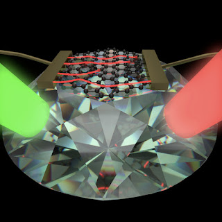
Graphene, a sheet of carbon just one atom thick, has a number of unique electronic properties, so it is ideal for fundamental studies in condensed matter physics and for making novel electronics and sensing devices. Researchers normally study the electron transport properties of graphene by measuring the material’s resistivity but this approach cannot make out variations in electronic properties caused by local structures, such as defects, which are very important in nanomaterials. Now, a team at the University of Melbourne in Australia has overcome this problem with their new technique based on quantum probes made from nitrogen-vacancy centres to image the flow of electric current in 2D nanomaterials like the carbon sheet - and has found that it is indeed disrupted by minute cracks and defects.
“Our technique is non-invasive, offers high sub-micron spatial resolution and works under ambient conditions,” explains lead author of the new study Jean-Philippe Tetienne. “It could be used to study electron transport in any atomically-thin materials and structures, which are especially vulnerable to imperfections like defects. This is important because it will allow us to see how electric currents are affected by these imperfections and so ultimately help us improve the reliability and performance of existing and emerging technologies.”
The new technique is based on a quantum sensing platform that consists of a diamond chip engineered with an array of atomic defects, known as nitrogen-vacancy (NV) centres. These centres, which form when a nitrogen impurity finds itself next to a missing carbon atom in the diamond lattice, are essentially tiny magnets and can be used as sensors for magnetic resonance imaging (MRI) at the nanoscale. This is because the spin of an electron associated with the NV is relatively insensitive to its environment thanks to the fact that diamond does not have a net nuclear spin.
Nanotechweb: NV-quantum probes measure electron flow in graphene, Belle Dumé

Comments