Topics: Consumer Electronics, Electrical Engineering, Materials Science, Nanotechnology
The MOSFET – Metal Oxide FET
 |
| Image Source: Electronics Tutorials |
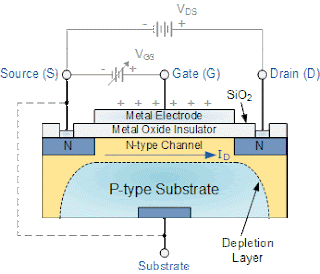
As well as the Junction Field Effect Transistor (JFET), there is another type of Field Effect Transistor available whose Gate input is electrically insulated from the main current carrying channel and is therefore called an Insulated Gate Field Effect Transistor or IGFET. The most common type of insulated gate FET which is used in many different types of electronic circuits is called the Metal Oxide Semiconductor Field Effect Transistor or MOSFET for short.
The IGFET or MOSFET is a voltage controlled field effect transistor that differs from a JFET in that it has a “Metal Oxide” Gate electrode which is electrically insulated from the main semiconductor n-channel or p-channel by a very thin layer of insulating material usually silicon dioxide, commonly known as glass. Source: Electronics Tutorials
 |
| By Appaloosa - Own work, CC BY-SA 3.0, https://commons.wikimedia.org/w/index.php?curid=10213475 |
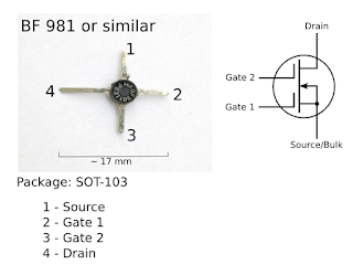
A multigate device or multiple gate field-effect transistor (MuGFET) refers to a MOSFET (metal–oxide–semiconductor field-effect transistor) which incorporates more than one gate into a single device. The multiple gates may be controlled by a single gate electrode, wherein the multiple gate surfaces act electrically as a single gate, or by independent gate electrodes. A multigate device employing independent gate electrodes is sometimes called a Multiple Independent Gate Field Effect Transistor (MIGFET). Multigate transistors are one of the several strategies being developed by CMOS semiconductor manufacturers to create ever-smaller microprocessors and memory cells, colloquially referred to as extending Moore's Law. Source: Wikipedia
 |
| Image Source: IEEE |
We demonstrate undoped-body, gate-all-around (GAA) Si nanowire (NW) MOSFETs with excellent electrostatic scaling. These NW devices, with a TaN/Hf-based gate stack, have high drive-current performance with NFET/PFET IDSAT = 825/950 μA/μm (circumference-normalized) or 2592/2985 μA/μm (diameter-normalized) at supply voltage VDD = 1 V and off-current IOFF = 15 nA/μm. Superior NW uniformity is obtained through the use of a combined hydrogen annealing and oxidation process. Clear scaling of short-channel effects versus NW size is observed. Additionally, we observe a divergence of the nanowire capacitance from the planar limit, as expected, as well as enhanced device self-heating for smaller diameter nanowires. We have also applied this method to making functional 25-stage ring oscillator circuits. Source: IEEE
Comments