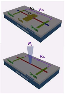
 |
| Image Source: MIT Technology Review |
Topics: Consumer Electronics, Electrical Engineering, Economy, Nanotechnology, Optics, STEM
This caught my eye working in the industry, especially since the doping of silicon or germanium substrates requires the introduction of impurities at high energies and many of them poisonous to humans, hence the great control we use in manufacture. My guess (or, my hope) is this will in some extent prove cleaner as well as cheaper to produce.
TECHNOLOGY REVIEW: The field effect transistor is the workhorse of the consumer electronics industry. Carved into microchips in the billions, these devices beaver away, more or less unnoticed, in practically every home, office, and laboratory in the developed world.
And yet there is a perennial problem with field effect transistors that keeps chip designers awake at night—how to make them ever smaller and thereby keep up the relentless pace of Moore’s Law.
These silicon layers have to be doped with other atoms—just a handful will do the trick in such small components. And therein lies the problem. Even small random variation in the number of dopant atoms in semiconductor components can have a huge effect on the behavior of the transistor. How to control these variations during manufacture is by no means clear. Then there is the physical problem of making a device with three terminals even smaller.
Today, Jason Marmon at University of North Carolina in Charlotte and a few pals unveil just such a device in the form of a light effect transistor. This is essentially a wire that conducts when it is bathed in light and insulates when it is dark. In other words, it is a switch modulated by light. The team says its new device is simpler than a field effect transistor and does not rely on dopant atoms, so it can be made smaller and thereby continue Moore’s law.
Abstract
Modern electronics are developing electronic-optical integrated circuits, while their electronic backbone, e.g. field-effect transistors (FETs), remains the same. However, further FET down scaling is facing physical and technical challenges. A light-effect transistor (LET) offers electronic-optical hybridization at the component level, which can continue Moore's law to the quantum region without requiring a FET's fabrication complexity, e.g. a physical gate and doping, by employing optical gating and photoconductivity. Multiple independent gates are therefore readily realized to achieve unique functionalities without increasing chip space. Here we report LET device characteristics and novel digital and analog applications, such as optical logic gates and optical amplification. Prototype CdSe-nanowire-based LETs show output and transfer characteristics resembling advanced FETs, e.g. on/off ratios up to ~1.0x10^6 with a source-drain voltage of ~1.43 V, gate-power of ~260 nW, and subthreshold swing of ~0.3 nW/decade (excluding losses). Our work offers new electronic-optical integration strategies and electronic and optical computing approaches.
Physics arXiv:
Light-effect transistor (LET) with multiple independent gating controls for optical logic gates and optical amplification
Jason K. Marmon, Satish C. Rai, Kai Wang, Weilie Zhou, Yong Zhang
Comments