nanotechnology (86)

Cyclocarbon...

5d568358294db.jpg
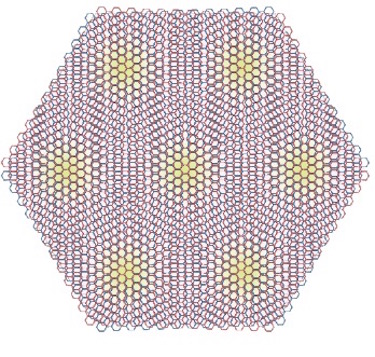
From left to right, precursor molecule C24O6, intermediates C22O4 and C20O2 and the final product cyclo [18]carbon C18 created on surface by dissociating CO masking groups using atom manipulation. The bottom row shows atomic force microscopy (AFM) data using a CO functionalized tip. Credit: IBM Research


Topics: Applied Physics, Atomic Force Microscopy, Chemistry, Nanotechnology, Research


A team of researchers from Oxford University and IBM Research has for the first time successfully synthesized the ring-shaped multi-carbon compound cyclocarbon. In their paper published in the journal Science, the group describes the process they used and what they learned about the bonds that hold a cyclocarbon together.

Carbon is one of the most abundant elements, and has been found to exist in many forms, including diamonds and graphene. The researchers with this new effort note that much research has been conducted into the more familiar forms (allotropes) how they are bonded. They further note that less well-known types of carbon have not received nearly as much attention. One of these, called cyclocarbon, has even been the topic of debate. Are the two-neighbor forms bonded by the same length bonds, or are there alternating bonds of shorter and longer lengths? The answer to this question has been difficult to find due to the high reactivity of such forms. The researchers with this new effort set themselves the task of finding the answer once and for all.

The team's approach involved creating a precursor molecule and then whittling it down to the desired form. To that end, they used atomic force microscopy to create linear lines of carbon atoms atop a copper substrate that was covered with salt to prevent the carbon atoms from bonding with the subsurface. They then joined the lines of atoms to form the carbon oxide precursor C24O6, a triangle-shaped form. Next, the team applied high voltage through the AFM to shear off one of the corners of the triangle, resulting in a C22O4 form. They then did the same with the other two corners. The result was a C18 ring—an 18-atom cyclocarbon. After creating the ring, the researchers found that the bonds holding it together were the alternating long- and short-type bonds that had been previously suggested.


Ring-shaped multi-carbon compound cyclocarbon synthesized, Bob Yirka , Phys.org

Read more…

Smart Packaging...

PWNANOApr18-pragmatIC-wafer-image.jpg
Cheaper flexible integrated circuits open up new markets. (Courtesy: PragmatIC)


Topics: Applied Physics, Moore's Law, Semiconductor Technology, Nanotechnology


For more than 50 years, progress in the electronics industry has been guided by Moore’s law: the idea that the number of transistors in a silicon-based integrated circuit (IC) will double approximately every 18 months. The consequences of this doubling include a continual reduction in the size of silicon ICs, as it becomes possible to provide increasingly complex and high-performance functionality in smaller and smaller areas of silicon, and at progressively lower cost relative to the circuits’ processing power.

Moore’s law is an empirical rule of thumb rather than a robust physical principle, and much has been written about how, why and when it will eventually fail. But even before we reach that point, manufacturers are already finding that, in practice, the cost savings associated with reducing the size, or “footprint”, of ICs will only carry them so far. The reason is that below a certain minimum size, ICs become difficult to handle easily or effectively. For highly complex circuitry, such as that found in computers with many millions of transistors in a single IC, this limit on handling size may not be a consideration. However, for applications that require less complex circuits, the size constraint imposed by the physical aspect of handling ICs becomes a limiting factor in their cost.

The approach we have taken at PragmatIC is to use thin, flexible substrates, rather than rigid silicon, as the base for building our circuits. The low cost of the materials involved and the relatively low complexity of our target applications alters the economics around circuit footprint and overall IC cost. Accepting a larger footprint can lower capital expenditure because it means that ultrahigh-end precision tooling is not required to fabricate our circuits during the manufacturing process. In turn, for low-complexity applications, this can lead to a lower final IC cost.

The resulting flexible integrated circuits, or FlexICs, are thinner than a human hair, so they can easily be embedded in everyday objects. They also cost around 10 times less than silicon ICs, making it economically viable for them to appear in trillions of smart objects that engage with consumers and their environments. Since the technology was developed, PragmatIC FlexICs have been trialed in a wide variety of markets, including consumer goods, games, retail, and the pharmaceutical and security sectors.


A smart approach to smart packaging
Catherine Ramsdale is vice-president of device development at PragmatIC

Read more…

TBG and Ferromagnets...

magic-angle.jpeg
Magic angle graphene superlattice. Scale=10 nm. Courtesy: P Jarillo-Herrero


Topics: Ferromagnetism, Graphene, Hall Effect, Magnetic Resonance Imaging, Nanotechnology


Researchers have found that electrons organize themselves into a new kind of ferromagnet in twisted bilayer graphene (TBG). In this system, which forms when two sheets of graphene are stacked on top of one another with a small twist angle between them, it is the orbital motion of electrons, rather than their spins, that aligns. Such behavior could produce emergent topological states that might be exploited in applications such as low-power magnetic memory in the future.

Graphene is a flat crystal of carbon just one atom thick. When two sheets of the material are placed on top of each other and misaligned by rotating them relative to each other, they form a moiré pattern. Last year, researchers at the Massachusetts Institute of Technology (MIT) found that at a “magic” twist angle of 1.1°, the material becomes a superconductor (that is, it can carry currents with no losses) at 1.7 K. This effect, which occurs thanks to miniband flattening at this angle that strongly enhances interactions between electrons in the material, disappears at slightly larger or smaller angle twists.

A team of researchers led by David Goldhaber-Gordon of Stanford University has now found unambiguous evidence of ferromagnetism – as the giant anomalous Hall (AH) effect – in TBG when its flat conduction miniband is three-quarters filled.


Ferromagnetism appears in twisted bilayer graphene, Belle Dumé, Physics World

Read more…

How We See the Small...

800px-AFM_used_cantilever_in_Scanning_Electron_Microscope_magnification_1000x.jpg
View of cantilever on an atomic force microscope (magnification 1000x).
Credit: SecretDisc GFDL, CC-BY-SA-3.0


Topics: Atomic Force Microscopy, Nanotechnology, Optics, Scanning Electron Microscope


Cell reproduction, disease detection and semiconductor optimization are just some of the areas of research that have exploited the atomic force microscope. First invented by Calvin Quate, Gerd Binnig and Christoph Gerber in the mid 1980s, atomic force microscopy (AFM) brought the atomic resolution recently achieved by the scanning tunnelling microscope to non-conducting samples, and helped to catalyse the avalanche of science and technology based on nanostructures that now permeates all aspects of modern life from smartphones to tennis rackets. On 6 July 2019 Calvin Quate died aged 95 at his home in Menlo Park, California.

Long before the development of AFM, Quate’s research had made waves in microscopy. 1978 had seen the announcement of the scanning acoustic microscope, which achieved the sensitivity of optical microscopy but probed samples so softly that it could image the interiors of living cells without damaging them. The technique uses high frequency sound waves in place of light, which penetrate deep into structures to image internal structures non-destructively. It is widely used in quality control of electronic component assembly among other applications such as printed circuit boards and medical products.
 

Advanced microscopy pioneer leaves broad ranging legacy
Anna Demming, Physics World

Read more…

Your iPhone as Tricorder...

Silicon chips similar to those that would be used in the detection process. Credit: Vanderbilt University/Heidi Hall


Topics: Applied Physics, Medical Physics, Nanotechnology, Star Trek


The simplest home medical tests might look like a deck of various silicon chips coated in special film, one that could detect drugs in the blood, another for proteins in the urine indicating infection, another for bacteria in water and the like. Add the bodily fluid you want to test, take a picture with your smart phone, and a special app lets you know if there's a problem or not.

That's what electrical engineer Sharon Weiss, Cornelius Vanderbilt Professor of Engineering at Vanderbilt University, and her students developed in her lab, combining their research on low-cost, nanostructured thin films with a device most American adults already own. "The novelty lies in the simplicity of the basic idea, and the only costly component is the smart phone," Weiss said.

"Most people are familiar with silicon as being the material inside your computer, but it has endless uses," she said. "With our nanoscale porous silicon, we've created these nanoscale holes that are a thousand times smaller than your hair. Those selectively capture molecules when pre-treated with the appropriate surface coating, darkening the silicon, which the app detects."


iPhone plus nanoscale porous silicon equals cheap, simple home diagnostics
Heidi Hall, Vanderbilt University, Phys.org

Read more…

SLIPS...

A novel, highly sensitive molecular sensor together with a first-of-its-kind histamine detector comprise abbieSense, a device that can diagnose and assess the severity of an allergic reaction within five minutes. Credit: Wyss Institute at Harvard University


Topics: Applied Physics, Fluid Mechanics, Microfluidics, Nanofluidics, Nanotechnology


The need for an inexpensive, super-repellent surface cuts across a vast swath of societal sectors—from refrigeration and architecture, to medical devices and consumer products. Most state-of-the-art liquid repellent surfaces designed in the last decade are modeled after lotus leaves, which are extremely hydrophobic due to their rough, waxy surface and the physics of their natural design. However, none of the lotus-inspired materials designed so far has met the mark: they may repel water but they fail to repel oils, fail under physical stress, cannot self-heal – and are expensive to boot.

‘SLIPS’ technology, inspired by the slippery pitcher plant that repels almost every type of liquid and solid, is a unique approach to coating industrial and medical surfaces that is based on nano/microstructured porous material infused with a lubricating fluid. By locking in water and other fluids, SLIPS technology creates slick, exceptionally repellent and robust self-cleaning surfaces on metals, plastics, optics, textiles and ceramics. These slippery surfaces repel almost any fouling challenge a surface may face—whether from bacteria, ice, water, oil, dust, barnacles, or other contaminants.


Wyss Institute, Harvard: Slippery Liquid Infused Porous Surfaces

Read more…