nanotechnology (84)

Blind Mice Seeing...

Figure

Topics: Bioengineering, Optical Physics, Nanorods, Nanotechnology

Even in the dark, rattlesnakes and their fellow pit vipers can strike accurately at small warm-blooded prey from a meter away. Those snakes, and a few others, can see in the IR—but not with their eyes. Rather, they have a pair of specialized sensory organs, called pit organs, located between their eyes and their nostrils and lined with nerve cells rich in temperature-sensitive proteins that cause the neurons to fire when heated.1 The pits work like pinhole cameras to focus incoming thermal radiation onto their heat-sensitive back walls; the thermal images are then superimposed with visual images in the snake’s brain.

Heat-responsive neurons are not unique to snakes. We have them over every inch of our skin, to feel objects warm to the touch, and on our tongues, to taste spicy food. But the snakes’ ability to resolve the source of radiated heat at a distance is unusual.

Inspired by the snakes, Dasha Nelidova and her colleagues at the Institute of Molecular and Clinical Ophthalmology in Basel, Switzerland, are developing a new treatment for forms of blindness caused by the degeneration of retinal photoreceptors.2 Using gene therapy, they endow remaining retinal cells with thermoresponsive proteins, thereby compensating for their lost light sensitivity with heat sensitivity. The proteins by themselves aren’t sensitive enough to rival normal vision, so the researchers tether them to gold nanorods, as shown in figure 1. The 80-nm-long nanorods strongly absorb near-IR light at 915 nm and convey the concentrated heat to the attached proteins.

Near-IR nanosensors help blind mice see, Johanna L. Miller, Physics Today

Read more…

Armored Surfaces...

233357_web.jpg
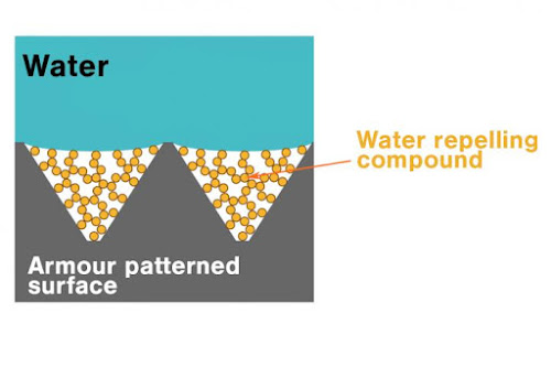
A schematic representation of how the surface looks, and how the structure repels water. Courtesy: Aalto University


Topics: Materials Science, Nanotechnology, Surface Engineering

A micron-scale “armor” that protects highly water-repellent nanostructures from damage has been developed by researchers in China and Finland. The new extra-durable coating could make it possible to employ these “superhydrophobic” surfaces on devices such as solar panels and vehicle windscreens that experience tough environmental conditions.

As their name suggests, superhydrophobic materials repel water extremely well. They owe this impressive ability to a thin layer of air that develops around nanometre-scale structures on their surface. By ensuring that droplets barely touch the solid part of the surface at all, the air layer effectively acts as a lubricant, allowing water droplets to roll off with near-zero friction.

These nanostructured surfaces are, however, mechanically fragile and can easily be wiped away. To address this drawback, a research team led by Xu Deng of the University of Electronic Science and Technology of China in Chengdu and Robin Ras of Finland’s Aalto University created a superhydrophobic surface containing structures at two different length scales: a nanoscale structure that is water repellent and a microscale one that provides durability.

The microstructure consists of an interconnected frame containing “pockets” of tiny inverted pyramids. Within these pyramids are the highly water-repellent and mechanically fragile nanostructures. The frame thus acts as a shield, preventing the nanostructure coating from being removed by abradants larger than the frame. “A finger, screwdriver or even sandpaper glides over these microstructures, leaving the nanostructures untouched, thereby preserving the surface’s attractive water-repellent feature,” Ras says.

Superhydrophobic surfaces toughen up, Isabelle Dumé, Physics World

Read more…

Comb on a Chip...


MoilleCover_v2-1.jpg
Experimental setup to generate a set of stable frequencies in a cryogenically cooled laser microresonator frequency comb. The ring-shaped microresonator, small enough to fit on a microchip, operates at very low laser power and is made from the semiconductor aluminum gallium arsenide.


Topics: Applied Physics, Instrumentation, NIST, Nanotechnology, Semiconductor Technology


Just as a meter stick with hundreds of tick marks can be used to measure distances with great precision, a device known as a laser frequency comb, with its hundreds of evenly spaced, sharply defined frequencies, can be used to measure the colors of light waves with great precision.

Small enough to fit on a chip, miniature versions of these combs — so named because their set of uniformly spaced frequencies resembles the teeth of a comb — are making possible a new generation of atomic clocks, a great increase in the number of signals traveling through optical fibers, and the ability to discern tiny frequency shifts in starlight that hint at the presence of unseen planets. The newest version of these chip-based “microcombs,” created by researchers at the National Institute of Standards and Technology (NIST) and the University of California at Santa Barbara (UCSB), is poised to further advance time and frequency measurements by improving and extending the capabilities of these tiny devices.

Comb on a Chip: New Design for ‘Optical Ruler’ Could Revolutionize Clocks, Telescopes, Telecommunications, NIST

Paper: G. Moille, L. Chang, W. Xie, A. Rao, X. Lu, M. Davanco, J.E. Bowers and K. Srinivasan. Dissipative Kerr Solitons in a III-V Microresonator. Laser and Photonics Reviews. June 2020. DOI: 10.1002/lpor.202000022

Read more…

2D Boost for 5G...

v5_Kim1a_green-724x1024.jpg
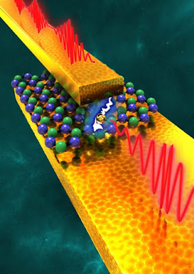
A diagram of the UT Austin team's switch showing two gold electrodes with a layer of hBN in between. (Courtesy: UT Austin)


Topics:  Boron Nitride, Internet of Things, Materials Science, Nanotechnology

Two-dimensional sheets of boron nitride can be used to create an analogue switch that gives communication devices more efficient access to radio, 5G and terahertz frequencies while increasing their battery life. The switch, which was developed by a team of researchers at the University of Texas at Austin in the US and the University of Lille in France, could be employed in a host of different applications, including smartphones, mobile systems and the “Internet of things”.

Analogue switches are routinely employed in communication systems to switch from one frequency band to another, route signals between transmitting and receiving antennas, and reconfigure wireless networks. Traditionally, these switches are based on solid-state diodes or transistors, but components of this type consume energy even in standby mode, reducing the battery life of the device. With 5G networking set to drive a tenfold increase in data throughput – enabling advances in self-driving cars, delivery drones, remote surgery and fast downloads of high-definition media in the process – addressing this energy drain is more urgent than ever.

5G switching gets a 2D boost, Isabelle Dumé, Physics World

Read more…

Photonic Nanojets...

5.0007611.figures.online.f1.jpeg
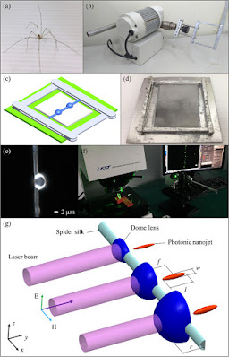
FIG. 1. (a) Long-legs cellar spider. (b) Reeling mechanism. (c) Manufacturing process of decorating spider silk. (d) Spider silk with dome lens placed on a dedicated holder. (e) Microphotograph of dome lens. (f) Laser scanning digital microscope system for measuring dome lens. (g) Schematic diagram of the dome lens for generating PNJ.


Topics: Biology, Materials Science, Nanotechnology

ABSTRACT

In this work, we thoroughly investigate the shape, size, and location of the photonic nanojets (PNJs) generated from the illuminated dome lens. The silk fiber is directly extracted from the cellar spider and used to form the dome lens by its liquid-collecting ability. The solidified dielectric dome lenses with different dimensions are obtained by using ultraviolet curing. Numerical and experimental results show that the long PNJs are strongly modulated by the dimension of the dome lens. The optimal PNJ beam shaping is achieved by using a mesoscale dielectric dome lens. The PNJ with a long focal length and a narrow waist could be used to scan over a target for large-area imaging. The silk fiber with a dome lens is especially useful for bio-photonic applications by combining its biocompatibility and flexibility.

Optimal photonic nanojet beam shaping by mesoscale dielectric dome lens

Journal of Applied Physics 127, 243110 (2020); https://doi.org/10.1063/5.0007611

C.B. Lin, Yi-Ting Lee, and Cheng-Yang Liu

Read more…

Greener Solar Cells...

49909461188_518f97cbf2_o.jpg
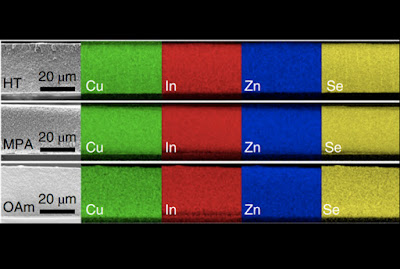
Scanning electron microscope image of electrodes infiltrated with quantum dots (left) and the corresponding distributions of copper, indium, zinc, and selenium across the film thickness. Courtesy: LANL


Topics: Green Tech, Nanotechnology, Quantum Mechanics, Solar Cells

Semiconducting nanocrystals called colloidal quantum dots (CQDs) are ideal for applications such as large-panel displays and photovoltaic cells thanks to their high efficiency and colour purity. Their main drawback is their toxicity, since they have traditionally been made from cadmium or other heavy metals, such as lead. Researchers at the Los Alamos National Laboratory in the US have now engineered cadmium-free QD solar cells that reach efficiencies on par with those of their environmentally-unfriendly counterparts. The key to the new devices’ high performance is their tolerance to defects, they say.

CQDs can be synthesized in solution, which means that films of these nanocrystals can be deposited quickly and easily on a range of flexible or rigid substrates – just like paint or ink. Such semiconducting nanocrystals are ideal for making highly-efficient inorganic solar cells that emit light via a process known as radiative recombination. Here, an electron in the valency energy band in the QD absorbs a photon and moves to the conduction band, leaving behind an electron vacancy, or hole. The excited electron and hole then recombine, releasing a photon.

The advantage of using CQDs as photovoltaic materials in solar cells is that they absorb light over a broad spectrum of solar radiation wavelengths. This is because the band gap of a CQD can be tuned over a large energy range by simply changing the size of the nanocrystals. Such a size-tuneable property has allowed the efficiencies of these QDs to rapidly approach those of traditional thin-film photovoltaics, such as PbS, CdTe and Pb-halide perovskite QDs.

Quantum dot solar cells get greener, Isabelle Dumé, Physics World

Read more…

"A Whole New Universe"...

d41586-020-01658-1_18045322.jpg
A Cryo-EM map of the protein apoferritin. Credit: Paul Emsley/MRC Laboratory of Molecular Biology


Topics: Biology, Cryogenic-Electron Microscopy, Materials Science, Nanotechnology

A game-changing technique for imaging molecules known as cryo-electron microscopy has produced its sharpest pictures yet — and, for the first time, discerned individual atoms in a protein.

By achieving atomic resolution using cryogenic-electron microscopy (cryo-EM), researchers will be able to understand, in unprecedented detail, the workings of proteins that cannot easily be examined by other imaging techniques, such as X-ray crystallography.

The breakthrough, reported by two laboratories late last month, cements cryo-EM’s position as the dominant tool for mapping the 3D shapes of proteins, say scientists. Ultimately, these structures will help researchers to understand how proteins work in health and disease, and lead to better drugs with fewer side effects.

“It’s really a milestone, that’s for sure. There’s really nothing to break anymore. This was the last resolution barrier,” says Holger Stark, a biochemist and electron microscopist at the Max Planck Institute for Biophysical Chemistry in Göttingen, Germany, who led one of the studies1. The other2 was led by Sjors Scheres and Radu Aricescu, structural biologists at the Medical Research Council Laboratory of Molecular Biology (MRC-LMB) in Cambridge, UK. Both were posted on the bioRxiv preprint server on 22 May.

“True ‘atomic resolution’ is a real milestone,” adds John Rubinstein, a structural biologist at the University of Toronto in Canada. Getting atomic-resolution structures of many proteins will still be a daunting task because of other challenges, such as a protein’s flexibility. "These preprints show where one can get to if those other limitations can be addressed,” he adds.

‘It opens up a whole new universe’: Revolutionary microscopy technique sees individual atoms for first time

Ewen Callaway, Nature

Read more…
Anna-Demming-4-May-2020.jpg
Next big thing:
Haifei Zhan and colleagues reckon that carbon nanothreads have a future in energy storage.
(Courtesy: Queensland University of Technology)


Topics: Applied Physics, Battery, Materials Science, Nanotechnology

Computational and theoretical studies of diamond-like carbon nanothreads suggest that they could provide an alternative to batteries by storing energy in a strained mechanical system. The team behind the research says that nanothread devices could power electronics and help with the shift towards renewable sources of energy.

The traditional go-to device for energy storage is the electrochemical battery, which predates even the widespread use of electricity. Despite centuries of technological progress and near ubiquitous use, batteries remain prone to the same inefficiencies and hazards as any device based on chemical reactions – sluggish reactions in the cold, the danger of explosion in the heat and the risk of toxic chemical leakages.

Another way of storing energy is to strain a material that then releases energy as it returns to its unstrained state. The strain could be linear like stretching and then launching a rubber band from your finger; or twisted, like a wind-up clock or toy. Over a decade ago, theoretical work done by researchers at the Massachusetts Institute of Technology suggested that strained chords made from carbon nanotubes could achieve impressive energy-storage densities, on account of the material’s unique  mechanical properties.

Diamond nanothreads could beat batteries for energy storage, theoretical study suggests

Anna Demmings, Physics World
Read more…

Open University...


gradient_img.png


Topics: Applied Physics, Education, Internet, Nanotechnology, STEM


Today poignantly, is the 50th anniversary of Earth Day. Some of us celebrate in willing self-isolation; others wish a repeat of the 1918 Influenza Pandemic by callously campaigning for others to die for an economy so wrought with inequality it cannot handle it's centennial equivalent.

A disclaimer note: Though these are unique times to say the least, this is not a support for fully online STEM education, though there can be some. Science for the most part is done in-person. I hope this is a bridge until we get to that again. It's hard to Zoom a breadboard circuit design or a laboratory set up.

Worldwide demand is growing for effective STEM (science, technology, engineering, and mathematics) education that can produce workers with technical skills. Online classes—affordable, flexible, and accessible—can help meet that demand. Toward that goal, some countries have developed national online higher-education platforms, such as XuetangX in China and Swayam in India. In 2015 eight top Russian universities collaborated to create the National Platform of Open Education, or OpenEdu. Professors from highly ranked departments produced courses for the platform that could then be used, for a fee, by resource-constrained universities. The courses comply with national standards and enable universities to serve more students by reducing the cost per pupil.

A new study from Igor Chirikov at the University of California, Berkeley, and his collaborators at Stanford and Cornell Universities and the National Research University Higher School of Economics in Moscow investigates the effectiveness of the OpenEdu program. The researchers looked at two metrics—effectiveness of instruction and cost savings—and found that the platform was successful on both fronts.


Online STEM courses can rival their in-person analogues
Christine Middleton, Physics Today

Read more…

So Much for Moore...

3nmpic1.png
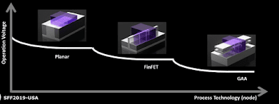
Figure 1: Planar transistors vs finFETs vs nanosheet FET. Source: Samsung


Topics: Applied Physics, Electrical Engineering, Moore's Law, Nanotechnology, Semiconductor Technology


So much for the Moore's law limit. Although under current circumstances, the progression might be stalled by our current viral situation: the cost of chips will go higher, and consumers are currently making choices on food, jobs and toilet paper, not gadgets.

Select foundries are beginning to ramp up their new 5nm processes with 3nm in R&D. The big question is what comes after that.

Work is well underway for the 2nm node and beyond, but there are numerous challenges as well as some uncertainty on the horizon. There already are signs that the foundries have pushed out their 3nm production schedules by a few months due to various technical issues and the unforeseen pandemic outbreak, according to analysts. COVID-19 has slowed the momentum and impacted the sales in the IC industry.

This, in turn, is likely to push back the roadmaps beyond 3nm. Nevertheless, the current climate hasn’t stopped the semiconductor industry. Today, foundries and memory makers are running at relatively high fab utilization rates.

Behind the scenes, meanwhile, foundries and their customers continue to develop their 3nm and 2nm technologies, which are now slated for roughly 2022 and 2024, respectively. Work is also underway for 1nm and beyond, but that’s still far away.

Starting at 3nm, the industry hopes to make the transition from today’s finFET transistors to gate-all-around FETs. At 2nm and perhaps beyond, the industry is looking at current and new versions of gate-all-around transistors.

At these nodes, chipmakers will likely require new equipment, such as the next version of extreme ultraviolet (EUV) lithography. New deposition, etch and inspection/metrology technologies are also in the works.

Needless to say, the design and manufacturing costs are astronomical here. The design cost for a 3nm chip is $650 million, compared to $436.3 million for a 5nm device, and $222.3 million for 7nm, according to IBS. Beyond those nodes, it’s too early to say how much a chip will cost.


Making Chips At 3nm And Beyond
Mark Lapedus and Ed Sperling, Semiconductor Engineering

Read more…

Silicon Sees the Light...

Hamish-8-April-2020-silicon-light-emitters-crop.jpg
Silicon sees the light: Elham Fadaly (left) and Alain Dijkstra in their Eindhoven lab. (Courtesy: Sicco van Grieken/SURF)


Topics: Optics, Electrical Engineering, Nanotechnology, Research, Solar Power, Spectroscopy


A light-emitting silicon-based material with a direct bandgap has been created in the lab, fifty years after its electronic properties were first predicted. This feat was achieved by an international team led by Erik Bakkers at Eindhoven University of Technology in the Netherlands. They describe the new nanowire material as the “Holy Grail” of microelectronics. With further work, light-emitting silicon-based devices could be used to create low-cost components for optical communications, computing, solar energy and spectroscopy.

Silicon is the wonder material of electronics. It is cheap and plentiful and can be fabricated into ever smaller transistors that can be packed onto chips at increasing densities. But silicon has a fatal flaw when it comes to being used as a light source or solar cell. The semiconductor has an “indirect” electronic bandgap, which means that electronic transitions between the material’s valence and conduction bands involve vibrations in the crystal lattice. As a result, it is very unlikely that an excited electron in the conduction band of silicon will decay to the valence band by emitting light. Conversely, the absorption of light by silicon does not tend to excite valence electrons into the conduction band – a requirement of a solar cell.


Silicon-based light emitter is ‘Holy Grail’ of microelectronics, say researchers
Hamish Johnston, Physics World

Read more…

Moore's Reckoning...

UMC_14nm_finfet.png
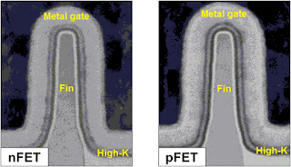
Wiki Chip: 14 nm lithography process


Topics: Electrical Engineering, Moore's Law, Nanotechnology, Semiconductor Technology


It was hard to tell at the time — with the distraction of the Y2K bug, the explosion of reality television, and the popularity of post-grunge music — that the turn of the millennium was also the beginning of the end of easy computing improvements. A golden age of computing, which powered intensive data and computational science for decades, would soon be slowly drawing to a close. Even with novel ways of assembling computing systems, and new algorithms that take advantage of the architecture, the performance gains as predicted by Moore’s law were bound to come to an end — but in a way few people expected.

Moore’s law is the observation that the number of transistors in dense integrated circuits doubles roughly every two years. Before the turn of the millennium, all a computational scientist needed to do to have more than twice as fast a computer was to wait two years. Calculations that would have been impractical became accessible to desktop users. It was a time of plenty, and many problems could be solved by brute-force computing, from the quantum interactions of particles to the formation of galaxies. Giant lattices could be modeled, and enormous numbers of particles tracked. Improved computers enabled the analysis of genomic variations in entire communities and facilitated the advent of machine-learning techniques in AI.

Fundamental physics limits will ultimately put an end to transistor shrinkage in Moore’s law, and we are close to getting there. Today, chip production creates structures in silicon that are 14 nanometers wide and decreasing, and seven-nanometer elements are coming to market. At these sizes, thousands of these elements would fit in the width of a human hair. Feature sizes of less than five nanometers will probably be impossible because of quantum tunneling, in which electrons undesirably leak out of such narrow gaps.


A Reckoning for Moore’s Law
Why upgrading your computer every two years no longer makes sense.
Ian Fisk, Simon's Foundation

Read more…

Interphase...

Battery%2BSeparator%2Band%2BElectrolyte.JPG
Intro to Nano Energy: Lecture 5


Topics: Battery, Materials Science, Nanotechnology


What happens in a lithium-ion battery when it first starts running? A complex series of events, it turns out – from electrolytic ion reorganization to a riot of chemical reactions. To explore this early part of a battery’s life, researchers in the US have monitored a battery’s chemical evolution at the electrode surface. Their work could lead to improved battery design by targeting the early stages of device operation.

The solid-electrolyte interphase is the solid gunk that materializes around the anode. Borne from the decomposition of the electrolyte, it is crucial for preventing further electrolyte degradation by blocking electrons while allowing lithium ions to pass through to complete the electrical circuit.

The solid-electrolyte interphase does not appear immediately. When a lithium ion battery first charges up, the anode repels anions and attracts positive lithium ions, separating oppositely charged ions into two distinct layers. This electric double layer dictates the eventual composition and structure of the solid-electrolyte interphase.


Emergence of crucial interphase in lithium-ion batteries is observed by researchers
Shi En Kim, Physics World

Read more…

Dilemma...

tech-dilemma.jpg
Green Book Blog: The Technology Dilemma, Zoë Dowling


Topics: Biology, Chemistry, COVID-19, Nanotechnology, Physics, Research, STEM


As the coronavirus outbreak roils university campuses across the world, early-career scientists are facing several dilemmas. Many are worrying about the survival of cell cultures, laboratory animals, and other projects critical to their career success. And some are reporting feeling unwelcome pressure to report to their laboratories—even if they don’t think it’s a good idea, given that any gathering can increase the risk of spreading the virus.

It’s unclear exactly how common these concerns are, but social media posts reveal numerous graduate students expressing stress and frustration at requests to come to work. “Just emailed adviser to say I am not comfortable breaking self isolation to come to lab this week. They emailed … saying I have to come in. What do I do?” tweeted an anonymous Ph.D. student on 16 March who doesn’t have essential lab work scheduled. “My health & safety should NOT be subject to the whims of 1 person. It should NOT be this scary/hard to stand up for myself.”

Many universities, including Harvard, have moved to shut down all lab activities except for those that are deemed “essential,” such as maintaining costly cell lines, laboratory equipment, live animals, and in some cases, research relating to COVID-19. But others have yet to ban nonessential research entirely.


Amid coronavirus shutdowns, some grad students feel pressure to report to their labs
Michael Price, Science Magazine, AAAS

I feel their pain.


The Scientific Method is very simple in concept:

Problem research - This involves gathering data in the form of previous written papers, published and peer-reviewed; writing notes (for yourself), summaries and reviews.

Hypothesis - This is your question asked from all the research, discussion with your adviser, especially if it's a valid question to ask or research to pursue.

Test the hypothesis - Design of experiment (s) to verify the hypothesis.

Data analysis - Usually with a software package, and a lot of statistical analysis.

Conclusion - Does it support the hypothesis?

- If so, retest several times, to plot an R squared fit of the data, so predictions can be made.

- If not, form another hypothesis and start over.

Often, conclusions are written up for peer review to be considered for journal publication. No one ever gets in on first submission - get used to rejection. Conclusions will be challenged by subject matter experts that may suggest other factors to consider, or another way to phrase something. Eventually, you get published. You can then submit an abstract to present a poster and a talk at a national conference.

Meeting Cancellation

It is with deep regret that we are informing you of the cancellation of the 2020 APS March Meeting in Denver, Colorado. APS leadership has been monitoring the spread of the coronavirus disease (COVID-19) constantly. The decision to cancel was based on the latest scientific data being reported, and the fact that a large number of attendees at this meeting are coming from outside the US, including countries where the CDC upgraded its warning to level 3 as recently as Saturday, February 29.


APS Physics: March.APS/about/coronavirus/


Update on Coronavirus

The health and safety of MRS members, attendees, staff, and community are our top priority. For this reason, we are canceling the 2020 MRS Spring Meeting scheduled for April 13-17, 2020, in Phoenix.

With our volunteers, we are exploring options for rescheduling programming to an upcoming event. We will share more information as soon as it becomes available.


MRS: Materials Research Society/2020-Spring Meeting


Social distancing and "shelter-in-place" slows the scientific enterprise. Science is in-person and worked out with other humans in labs and libraries. However, I am in support of this action and reducing the impact on the healthcare industry that on normal days are dealing with broken bones, gunshot wounds; cancer and childbirth surgeries with anxious, expectant mothers.

The dilemma is the forces that would reject the science behind this pandemic (and most science in any endeavor), would have us all "go back to work" after two weeks. The curve we're trying to flatten could sharply spike. The infection rates would increase and otherwise healthy people would be stricken. Immunodeficient groups would start getting sick again ...dying again. Our infrastructure is not designed for that many sick or dead people. Science continues with our survival and societal stability.

The persons with the solutions might be chomping-at-the-bit at home for now. Survival insures science will continue ...someday.
Read more…
187839_web.jpg
CAPTION
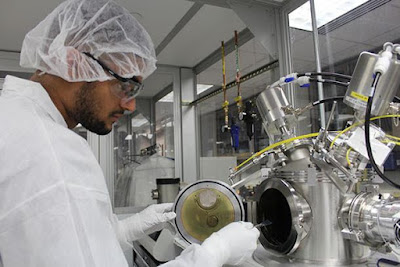
A graduate student gains hands-on experience with state-of-the-art nanotechnology equipment in the Center for Nanotechnology Education and Utilization Teaching Cleanroom.

CREDIT
Penn State


Topics: African Americans, Diversity, Diversity in Science, Existentialism, Nanotechnology, STEAM

Related: Be Thankful for What You Got, William DeVaughn, Genius Lyrics


Note: When this post appears, I will be in a midterm in Solid State Devices. I purposely did not post yesterday to let the tribute to Ms. Katherine Johnson Tuesday be an appropriate and respectful dénouement. After Friday seminar, I will take a needed spring break.

Nanotechnology is STEM at the 10-9 meter scale: a nanometer. To advance any understanding at that level, there has to be a respect for objective truth:

A proposition is considered to have objective truth when its truth conditions are met without bias caused by a sentient subject. Scientific objectivity refers to the ability to judge without partiality or external influence, sometimes used synonymous with neutrality. Wikipedia

After Watergate, a political party created its own echo chamber in print, radio, television and the Internet that now confuses objective versus subjective truth, i.e. that which matters in ones own opinion is therefore defended as "fact." We're daily inundated with the solipsistic subjective truth of a pathological liar, which that in and of itself is an area of mental illness as democracy is not a matter of "opinion," but a debate over a shared view of facts and what if anything will be done to ameliorate any problem put forwards. Ostrich politics doesn't even work for ostriches: like most foul, their not burying their heads in sand, they eat it and gravel to aid with their digestion.

Raking and mopping will not address climate change; neither will denying the spreading of the coronavirus in the west. It doesn't help that funding for the CDC and HHS were cut, and a lot of government agencies designed to fight pandemics either shuttered, unfunded or both. Forgive me if I'm dubious that the party whose senator brings a snowball to the well of the senate to disprove climate change won't eventually cut what we could innovate in nanotechnology, particularly expanding it to underrepresented groups to participate. They wouldn't see the value it gives to all Americans because they are just that myopic.

November 3, 2020 might as well be Judgment Day, when we either right this ship of state from the impact of ignoramuses and "alternative facts," or this dark momentum will edge us over the precipice into dystopia. Once America falls - and I'm sure her enemies know this - all other democracies around the world and civilization, is in peril.

Like the right wing truckers with smokestacks to "own the libs": we all have to live on the same planet: cooperation, or extinction.


*****


New Louis Stokes Regional Center of Excellence created with National Science Foundation funding

Traditionally, minority students have been underrepresented in science, technology, engineering and mathematics (STEM) programs -- and in the STEM marketplace. And as the U.S. innovation economy continues to grow, there comes an increasing requirement for skilled STEM workers to maintain the nation's status as a global leader. However, a significant challenge for workforce diversity exists because of limited access to underrepresented populations to quality STEM education and opportunities for STEM employment.

To try and overcome this challenge and ensure national competitiveness and sustained STEM global leadership, the Penn State Center for Nanotechnology Education and Utilization (CNEU), along with Norfolk State University (NSU) and Tidewater Community College (TCC), will form the Southeastern Coalition for Engagement and Exchange in Nanotechnology Education (SCENE) Louis Stokes Regional Center of Excellence in Broadening Participation. A total of $1.2 million in funding for this center was recently awarded by the National Science Foundation.

SCENE will focus on increasing recruitment and retention of underrepresented minority (URM) undergraduate and graduate students at Historically Black Colleges and Universities (HBCU) and at community colleges with minority and underrepresented student enrollments. Recruitment efforts will be aimed at students studying STEM through nanoscience and nanotechnology education and engagement.


Nanotechnology center to help broaden participation of minorities in STEM fields
6 December 2018, Penn State


SO let us summon a new spirit of patriotism; of service and responsibility where each of us resolves to pitch in and work harder and look after not only ourselves, but each other. Let us remember that if this financial crisis taught us anything, it’s that we cannot have a thriving Wall Street while Main Street suffers – in this country, we rise or fall as one nation; as one people.

We Rise and Fall as ONE Nation, November 5, 2008, President-elect Barack Obama, New York Post

"We must learn to live together as brothers or perish together as fools." Dr. Martin Luther King, Jr.
Read more…

A Beautiful Life...

nyTc9e3BK5fDLDSL26csHT-650-80.jpg
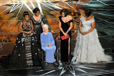
NASA mathematician Katherine Johnson (second left) is honored onstage with actors (left to right) Janelle Monae, Taraji P. Henson and Octavia Spencer - the stars of "Hidden Figures," which focuses on Johnson's work with NASA's Mercury program - during the 89th Annual Academy Awards at Hollywood & Highland Center on February 26, 2017 in Hollywood, California. NASA astronaut Yvonne Cagle is seen standing behind Johnson
(Image: © Kevin Winter/Getty Images) Space.com

Topics: African Americans, Diversity, Diversity in Science, Nanotechnology, NASA, Women in Science


Despite segregation, setbacks and Jim Crow, Katherine Johnson is one of the many "shoulders of giants" we stand upon.

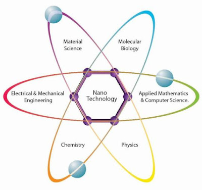
As alluded to yesterday, nanotechnology is multifaceted: molecular biology, materials science, electrical and mechanical engineering, chemistry and physics. Her specific area was applied mathematics and computer science, without which no data could be analysed post an experiment.

That's what women were called back then: computers. Computer mainframes were just beginning development, the transistor - discovered by William Shockley, John Bardeen and Walter Houser Brattain - was exploited to reduce payload by the nascent NASA to win the space race against the Russians who launched Sputnik. The spin off from that effort was codified in Moore's law that has given us everything from flash drives to smart phones. The foundation of all this is mathematics - paper, pencil, chalk or dry erase board. The answer sometimes has to be wrestled with and ground out. From the calculus step, one typically encounters an impressive breadth of algebra to wade through.

I particularly thought of Ms. Johnson on a MATLAB (matrix laboratory) assignment coding the Euler equation. Though daunting, my code successfully executed what I asked of it. I did it in the 21st century, where I did not have the indignity of bathrooms designated based on my skin color or gender. I have you, my sister and many other giants to thank for that.

The two things I can say that are most appropriate and respectful to Ms. Johnson's family in this time of their loss:

Thank you.
Godspeed.


HAMPTON, Va. (AP) — NASA says Katherine Johnson, a mathematician who worked on NASA’s early space missions and was portrayed in the film Hidden Figures, about pioneering black female aerospace workers, has died.

In a Monday morning tweet, the space agency said it celebrates her 101 years of life and her legacy of excellence and breaking down racial and social barriers.


Pioneering NASA mathematician Katherine Johnson of ‘Hidden Figures’ fame has died at 101
The Associated Press on TheGrio.com

#P4TC links:

Admiration and Gratitude...August 27, 2018
Modern Figures 28 February 2017...February 28, 2017
Katherine Johnson...February 2, 2018
Euler's Method...January 17, 2017
Hidden Figures...January 6, 2017

Read more…

Article 1 Section 8 | Clause 8...

blog-omni-nano-how-to-define-nanotechnology-001.jpg
Image Source: Omni Nano - The challenge of defining nanotechnology to a broad audience


Topics: African Americans, Diversity, Diversity in Science, Nanotechnology


Article I Section 8 | Clause 8 – Patent and Copyright Clause of the Constitution. [The Congress shall have power] “To promote the progress of science and useful arts, by securing for limited times to authors and inventors the exclusive right to their respective writings and discoveries.”


Stanford University Libraries: Fair Use/US Constitution


This is the least-mentioned clause in The Constitution. We tend to get in a twist over the First and Second Amendments (likely not because of the importance of every amendment, but that these are the first two, and most discussed popularly).

About the NNI

Welcome to the National Nanotechnology Initiative (NNI) website. The NNI is a U.S. Government research and development (R&D) initiative involving 20 departments and independent agencies working together toward the shared vision of "a future in which the ability to understand and control matter at the nanoscale leads to a revolution in technology and industry that benefits society." The NNI brings together the expertise needed to advance this broad and complex field—creating a framework for shared goals, priorities, and strategies that helps each participating Federal agency leverage the resources of all participating agencies. With the support of the NNI, nanotechnology R&D is taking place in academic, government, and industry laboratories across the United States.


NANO.gov: About the NNI


What is the NNI?

The NNI is a U.S. Government research and development (R&D) initiative involving the nanotechnology-related activities of 20 departments and independent agencies. The United States set the pace for nanotechnology innovation worldwide with the advent of the NNI in 2000. The NNI today consists of the individual and cooperative nanotechnology-related activities of Federal agencies with a range of research and regulatory roles and responsibilities. Funding support for nanotechnology R&D stems directly from NNI member agencies. As an interagency effort, the NNI informs and influences the Federal budget and planning processes through its member agencies and through the National Science and Technology Council (NSTC). The NNI brings together the expertise needed to advance this broad and complex field—creating a framework for shared goals, priorities, and strategies that helps each participating Federal agency leverage the resources of all participating agencies. With the support of the NNI, nanotechnology R&D is taking place in academic, government, and industry laboratories across the United States.


NANO.gov: What is the NNI?


"To promote the progress of science and useful arts,"...

This shouldn't be left up to interpretation, but science and useful arts is an instructive turn of phrase.

Useful art, or useful arts or techniques, is concerned with the skills and methods of practical subjects such as manufacture and craftsmanship. The phrase has now gone out of fashion, but it was used during the Victorian era and earlier as an antonym to the performing art and the fine art. Wikipedia/Useful_art

Creationism/Intelligent Design/Flat and Young Earth enthusiasts are not advocating science: they're  pseudoscience. Like eugenics, it is the counter authoritarianism gives when it feels threatened. If some of its proponents have patents, I am not aware, but if they possess them, they adhered to STEM disciplines, not poppycock.

The United States has an undistinguished history built on the foundations of land theft from First Nation Peoples (so-called Indians by Columbus) and involuntarily enslaved Africans of the Diaspora.

This however is the invention clause that awards patents for creative ideas, documenting its originator, how the invention is used and ownership. Inventions create commerce, jobs and most importantly: wealth.

The website Interesting Engineering: The A-Z List of Black Inventors is probably not an all-encompassing list, numbering 248. However, it should be a guide to how and where African Americans have contributed through their inventiveness to society and this nation. Cautionary at casual observance, it suggests the problems of the community is merely a matter of chutzpah and bootstraps.

Although Jasper Newton “Jack” Daniel is credited with inventing Jack Daniel’s in the 19th century, the company revealed last year that Daniel learned the trade of whiskey making from a slave named Nathan “Uncle Nearest” Green. (Green’s nickname is often incorrectly misspelled as “Nearis.”) Daniel then went on to open the Jack Daniel’s Tennessee whiskey distillery in 1875, where Green worked as the master distiller until at least 1881.

New York Times best-selling author Fawn Weaver says she discovered the story of Green from an article published by The New York Times that moved her to dig more into his history. That’s when she learned that Green was not the only African American involved in the process of distilling Jack Daniel’s whiskey. In fact, generations of Green’s descendants worked together with the Daniel family to make the iconic whiskey decades later. Some of Green’s offspring still work in the whiskey industry today.


THE SLAVE BEHIND JACK DANIEL’S WHISKEY RECIPE TO RECEIVE NEW HONOR
Selena Hill, Black Enterprise, July 28, 2017


This issue has always been fair use, and fairness.

What impact would fairness have had on the Green family with complete patent control of what has now become an American icon?

According the Center for American Progress in an article written by Angela Hanks, Danyelle Solomon, and Christian E. Weller in 2018, the median wealth of black and white in America will not come to equivalency for 200 years. That is a byproduct not of preponderance of Melanin or assigned depravity: it was government policy, hubris and ignorance on the Greens' part as to what rights they had to their invention.

..."by securing for limited times to authors and inventors the exclusive right to their respective writings and discoveries."

Whatever creativity, inventive ideas we contribute in macro, micro or nano spaces, may we be treated fairly; allowing us the fair use of "science and useful arts" towards the benefit of mankind, our progeny and posterity. Such may narrow the 200 years predicted, the equivalent of starting a 100 meter dash in leg irons.
Read more…

Current Time...

drake-equation-1600px.jpg
The Drake Equation from the SETI institute.


Topics: African Americans, Drake Equation, Existentialism, Extinction, Nanotechnology, Philosophy

Where:

N = The number of civilizations in the Milky Way Galaxy whose electromagnetic emissions are detectable.
R* = The rate of formation of stars suitable for the development of intelligent life.
fp = The fraction of those stars with planetary systems.
ne = The number of planets, per solar system, with an environment suitable for life.
fl = The fraction of suitable planets on which life actually appears.
fi = The fraction of life bearing planets on which intelligent life emerges.
fc = The fraction of civilizations that develop a technology that releases detectable signs of their existence into space.
L = The length of time such civilizations release detectable signals into space.

*****

Note: This milestone will be one month old Sunday. We shaved 20 seconds.

Closer than ever:
It is 100 seconds to midnight
2020 Doomsday Clock Statement

Science and Security Board
Bulletin of the Atomic Scientists

Editor, John Mecklin


Editor’s note: Founded in 1945 by University of Chicago scientists who had helped develop the first atomic weapons in the Manhattan Project, the Bulletin of the Atomic Scientists created the Doomsday Clock two years later, using the imagery of apocalypse (midnight) and the contemporary idiom of nuclear explosion (countdown to zero) to convey threats to humanity and the planet. The decision to move (or to leave in place) the minute hand of the Doomsday Clock is made every year by the Bulletin’s Science and Security Board in consultation with its Board of Sponsors, which includes 13 Nobel laureates. The Clock has become a universally recognized indicator of the world’s vulnerability to catastrophe from nuclear weapons, climate change, and disruptive technologies in other domains.


To: Leaders and citizens of the world
Re: Closer than ever: It is 100 seconds to midnight
Date: January 23, 2020


Humanity continues to face two simultaneous existential dangers—nuclear war and climate change—that are compounded by a threat multiplier, cyber-enabled information warfare, that undercuts society’s ability to respond. The international security situation is dire, not just because these threats exist, but because world leaders have allowed the international political infrastructure for managing them to erode.

In the nuclear realm, national leaders have ended or undermined several major arms control treaties and negotiations during the last year, creating an environment conducive to a renewed nuclear arms race, to the proliferation of nuclear weapons, and to lowered barriers to nuclear war. Political conflicts regarding nuclear programs in Iran and North Korea remain unresolved and are, if anything, worsening. US-Russia cooperation on arms control and disarmament is all but nonexistent.

Public awareness of the climate crisis grew over the course of 2019, largely because of mass protests by young people around the world. Just the same, governmental action on climate change still falls far short of meeting the challenge at hand. At UN climate meetings last year, national delegates made fine speeches but put forward few concrete plans to further limit the carbon dioxide emissions that are disrupting Earth’s climate. This limited political response came during a year when the effects of man-made climate change were manifested by one of the warmest years on record, extensive wildfires, and quicker-than-expected melting of glacial ice.

Continued corruption of the information ecosphere on which democracy and public decision making depend has heightened the nuclear and climate threats. In the last year, many governments used cyber-enabled disinformation campaigns to sow distrust in institutions and among nations, undermining domestic and international efforts to foster peace and protect the planet.

This situation—two major threats to human civilization, amplified by sophisticated, technology-propelled propaganda—would be serious enough if leaders around the world were focused on managing the danger and reducing the risk of catastrophe. Instead, over the last two years, we have seen influential leaders denigrate and discard the most effective methods for addressing complex threats—international agreements with strong verification regimes—in favor of their own narrow interests and domestic political gain. By undermining cooperative, science- and law-based approaches to managing the most urgent threats to humanity, these leaders have helped to create a situation that will, if unaddressed, lead to catastrophe, sooner rather than later.


*****


The full PDF version of the above is here. Facebook has finally released limited data for social scientists to research the effect of their platform on democracy, just as our senate blocks bills meant for protecting the voting franchise. State legislatures in Florida and Georgia make it difficult for ex-felons or people of color to vote - who needs Russians when shortsighted republicans will do? The confluence of avarice and racist hegemony may well spell the epitaph of our republic, species, and life on this planet. The 2020 elections may slow the Doomsday Clock, or speed us seconds closer.

In the Drake Equation, that even Dr. Frank Drake hedges bets against, the L: the length of time such civilizations release detectable signals into space, along with the fraction of planets where intelligent life emerges (I'm dubious about ours) are the most important variables in the equation, from a philosophical point of view.

It means to me: no more Ginai Seabron graduates, no nanoscience, nanoengineering or nanotechnology. No fretting about how to make the discipline inclusive, as surviving cavemen and women have other more pressing concerns. There cannot be advancement on such an aggressive act of mutually-assured destruction (M.A.D.). There are no "winners" or losers following such a destructive path, only un-buried corpses.

It means to me: if we survive our own avarice and hubris, my granddaughter can have a future not decided by "the color of her skin, but by the content of her character," and she could literally reach for the stars. Or, we could all be baited to Armageddon by a tweet. You can apparently get reduced sentences for your friends, despite DOJ guidelines. A Banana Republic in 140 characters. "Stop and frisk"; non-disclosure agreements for sexual harassment from the so-called benign (actual) billionaire candidate doesn't give me much hope. For my granddaughter's future, I'd like to have some.

We would theoretically and literally, then all be equalized to ashes. The universe would be indifferent to which pile of ash was a billionaire or pauper, so-called white, black or other; or a grandfather making his granddaughter laugh with a silly song about "little feet." Our self-induced inequality problems would be solved - for eternity.

The search for extraterrestrial intelligence would be over on our end, as earthbound intelligence, post-Apocalypse would then have been found...bereft.
Read more…

Ginai Seabron...

Ginai%2BSeabron.jpg
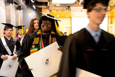
Ginai Seabron smiles as she exits the Biocomplexity Institute at Steger Hall after the nanoscience graduation ceremony, held the afternoon of May 11.


Topics: Diversity, Diversity in Science, Nanotechnology, Women in Science


On May 11, (2018) Ginai Seabron became the first African-American woman to earn a B.S. in nanoscience from the College of Science at Virginia Tech.

As one of only 20 graduating seniors in the nanoscience major, which is part of the college's Academy of Integrated Science, Seabron accepted her degree at the Biocomplexity Institute in Steger Hall among shouts of support and cheers from her peers, friends, and family.

Social media has proven that more than just her personal connections are proud of her accomplishment.

“I didn’t expect it at all,” Seabron said of her post going viral. “It’s overwhelming, but I love it.”

Hours before commencement, Seabron spoke through tears as she reflected on her Virginia Tech experience.

“It is not easy at all being the only African-American in the room,” she said. “It’s intimidating.”

She chose not to give up, and in doing so inspired others to pursue the degree. “I’ve actually helped a few other people in my black community transfer into the nanoscience department.”

Her advice to future students comes from lessons she’s learned along the way.

“Continue to push,” she said. “Rely on your family and your friends. Reach out to your professors. Go to office hours. Create your own office hours if you have to. Be social. Step out of your comfort zone. Get to know the people in your class — they could become your study buddies. You’ll think you’re the only person struggling, but as it turns out, everybody’s struggling.”


Virginia Tech graduate becomes first African-American woman to earn degree in nanoscience

*****

I dream a world where man
No other man will scorn,
Where love will bless the earth
And peace its paths adorn
I dream a world where all
Will know sweet freedom's way,
Where greed no longer saps the soul
Nor avarice blights our day.
A world I dream where black or white,
Whatever race you be,
Will share the bounties of the earth
And every man is free,
Where wretchedness will hang its head
And joy, like a pearl,
Attends the needs of all mankind-
Of such I dream, my world!

Langston Hughes, I Dream A World, All Poetry dot com

Read more…

Dr. Moddie Taylor...

Moddie-Taylor-courtesy-Smithsonian-300x237.jpg
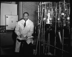
Dr. Moddie Taylor, Smithsonian


Topics: African Americans, Chemistry, Diversity in Science, Nanotechnology


Moddie Taylor was born on this date March 3, 1912. He was an African American chemist.

From Nymph, Alabama, Moddie Daniel Taylor was the son of Herbert L. Taylor and Celeste (Oliver) Taylor. His father worked as a postal clerk in St. Louis, Missouri, and it was there that Taylor went to school, graduating from the Charles H. Sumner High School in 1931. He then attended Lincoln University in Jefferson City, Missouri, and graduated with a B.S. in chemistry in 1935 as valedictorian and as a summa cum laude student. He began his teaching career in 1935, working as an instructor until 1939 and then as an assistant professor from 1939 to 1941 at Lincoln University, while also enrolled in the University of Chicago's graduate program in chemistry. He received his M.S. in 1939 and his Ph.D. in 1943.

Taylor married Vivian Ellis on September 8, 1937, and they had one son, Herbert Moddie Taylor. It was during 1945 that Taylor began his two years as an associate chemist for the top-secret Manhattan Project based at the University of Chicago. Taylor's research interest was in rare earth metals (elements which are the products of oxidized metals and which have special properties and several important industrial uses); his chemical contributions to the nation's atomic energy research earned him a Certificate of Merit from the Secretary of War. After the war, he returned to Lincoln University until 1948 when he joined Howard University as an associate professor of chemistry, becoming a full professor in 1959 and head of the chemistry department in 1969.

In 1960, Taylor's First Principles of Chemistry was published; also in that year the Manufacturing Chemists Association as one of the nation’s six top college chemistry teachers selected him. In 1972, Taylor was also awarded an Honor Scroll from the Washington Institute of Chemists for his contributions to research and teaching. Taylor was a member of the American Chemical Society, the American Association for the Advancement of Science, the National Institute of Science, the American Society for Testing Materials, the New York Academy of Sciences, Sigma Xi, and Beta Kappa Chi, and was a fellow of the American Institute of Chemists and the Washington Academy for the Advancement of Science. Taylor retired as a professor emeritus of chemistry from Howard University on April 1, 1976, and died of cancer in Washington, D.C., on September 15, 1976.


African American Registry: Dr. Moddie Taylor

Read more…